I guess if using an attenuator on the output of the 5102 you could do away with the second series resistor and connect the resistor to ground in parallel to the capacitor, which in turn can be scaled to the remaining series resistor. In my case Icm not concerned about chasing the last bit as using it as a rack mount stans alone unit with amps having different input requirements. I thn use limiters in the DSP to stop any chance of clipping the maps outputs.
Hadn't noticed the clock requirements re 96K, have only run mine at 48K but was going to set 64x oversampling to be able to use 96k.
Currently reconsidering building a pcb with an adau chip as opposed to going with an aliexpress core board, as jlcpcb minimum order is 5 units, could get expensive fast if I screw up.
Don´t have to be expensive at all;
For 4 layer, keep the design smaller than 10x10 cm (only 7 usd for 5 pcs)
Use only (or as much as at all possible) what they call basic components. Extended components cost 3 usd extra pr type to mount
Minimum no of pcb is 5 but minimum number of populated pcbs is only 2.
If it's the first board; keep it simple 😉
Yes we all screw up, but that is called learning 😉 .... my firs ADAU1701 bord I had somehow gotten 2 pins swhiched around ... didn't work .... come again 🙂
Yes might also skip the output attenuator and just use limiter function to keep below the rated sensivity ....
Thanks, I thought it was a minimum of 5, not sure I'll manage 10x10 though with the headers for esp32 and cypress programmer, may build the cypress directly onto the board though as that won't change.
They actually have the Cypress chip on stock. Have also considered this option, but it also requires a crystal and a eeprom. Another question is how to program the Cypress eeprom to start out with?
On the other hand you also only use the programming from time to time when you want to change something, so it's not much of a hassle to use a separate programmer I think .. and it adds mote then 10 usd to the build.
I which there was a programmer based on something much smaller and simple .... seems like overkill to use the cypress 8051 type, meaning way too many pins and needing both a crystal and an eeprom off chip
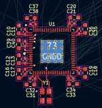

Getting there .... schematics sort of finished. Found a few mistakes, but need further review.
Placement done according to schematics v0.9
Routing 10% done
Was able to reduce size to 100 x 80 mm
Placement done according to schematics v0.9
Routing 10% done
Was able to reduce size to 100 x 80 mm
Attachments
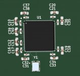
Was almost finished with the layout ... but my placement was not very good for separating GNDA and GNDD.
Unrouted it all and did a new placement with all analog stuff to one side. The ADCs and DACs are made so one side is analog and the other is digital, so having a split down through is easy to implement.
Let's see how the routing works out on second attempt.
Note: Again I'm really happy with KiCad 6.0, can't what it should be missing.
Found a trick yesterday: Use the "Edit Symbol Fields.." under Tools in Schematics to easily change and copy foot prints from one component to another ... really need feature, if you have placed a lot of components and realize you need to change some or all footprints ... I had used the "hand solder" versions of the resistors and caps, and wanted to change for the regular and smaller type ... took only 2 min
Attachments
Forgot to mention re programming of Cypress USBI: https://www.diyaudio.com/community/...-using-cypress-cy7c68013a-board.269111/page-3
In an earlier post you mention resistors on the mclk lines to reduce ringing, I think it more of a case of considering them as transmission lines and the resistors are used to damp reflections from the ends of the line, I'm planning on a single resistor as close to source as possible and then fan out from there with even length lines.
Your way ahead of me on your board, I'm still on the PCM chips and part done the power section.
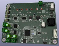
4 differential inputs with anti aliasing and CMRR filters, 8 pseudo balanced out, 48V (phantom power protected).

In an earlier post you mention resistors on the mclk lines to reduce ringing, I think it more of a case of considering them as transmission lines and the resistors are used to damp reflections from the ends of the line, I'm planning on a single resistor as close to source as possible and then fan out from there with even length lines.
Your way ahead of me on your board, I'm still on the PCM chips and part done the power section.
4 differential inputs with anti aliasing and CMRR filters, 8 pseudo balanced out, 48V (phantom power protected).
Looks Good SubSoniks
Lot's of electrolytic caps. Is that really necessary?
I'm planning on only using 10uF 0603 X5R + 100 nF X7R 0402 for all decoupling. Need to make an estimate of the total impedance vs freq to get a feel for where the max peaks are situated in frequency, to make sure it is not coinciding with any of the switching frequencies.
One thing to consider I think is the longevity of the caps. Chip caps would last "forever", cheaper el caps .... long but not forever
Is the Caps in input e.g. C11, C12 two caps in bipolar config?
Don't know if you get good bipolar caps as smd, but there are some good choices leaded, e.g. Muse, or Nichicon VP series ... uses less space on the board
What ADCs are you using?
DAC looks like PCM5102A 😉
Yes, PCM5102 for the DACs and PCM1802 ADCs.
Starting at the inputs, all C0G/NP0 filter caps for in the analogue path except for Panasonic FC 47uF in bipolar config (block 48V in and the 2.5 bias from the ADC), the FC caps are also used for the DAC outputs and the switching regulator.
I have used 10uF Nichicon (not low ESR) electrolytics combined with a small X7Rs for the ADC and DAC bypass, originally had all ceramics but after some checking it seemed to make sense to go with a combination, theory goes? that the the higher ESR would help damp potential resonances and also swamp the piezo effect of the smaller MLCC, I haven't gone so far as to calc the resonances and for this build will take my chances I think, hoping that the Nichicons will damp them down, hopefully...
The switcher I nabbed from your BOM 🙂
Rail voltages are: 12V main supply > Switcher - 6.7V > 3 x 5V (1 x 5VA, 1x5VD, 1x5V aux) > 3VA, 3VD and maybe a second 5VD I/O for the DSP.
Regs are LDL1117 ST, MLCC friendly using the recommended X7R values. I went with 1206 size as it looks like the larger package size have a more stable capacitance over a range of voltages.
I think I'm also going to go with this new layout scheme to reduce the I2S track lengths.
Regs in the top right are the 5VA for the ADCs, the second drops the 5VA to 3.3VA for the analogue supply side of the DACs.
Maybe it's my eyes deceiving me but your PCM1802 footprints looks quite narrow (compared to the PCM5102).
The casing on JLCPCB is the SSOP (DB) | 20 ..... I'll check my own board ... might be me
PCM5102A uses TSSOP (PW) | 20
I'm not so concerned by equal length of the I2S lines btw the different ICs, for the DACS it will not matter if the 4 chips are in total sync, as the output is analog. For the ADCs I hope and trust it will be corrected by the DSP interface (as it is the Master). As long at the clock is the same between them
Last edited:
For transferring caps, take a look here:
https://www.diyaudio.com/community/...lar-caps-measured-120db-thd-140db-imd.270676/
-120 db .... not significant for a ADC like PCB1802
https://www.diyaudio.com/community/...lar-caps-measured-120db-thd-140db-imd.270676/
-120 db .... not significant for a ADC like PCB1802
Phew, well spotted, I have used the wrong footprint, mistake due to easyeda library not having the part in the program but is available in the jlcpcb pcb manufacture library (but no footprint in the parts library) so had copied another as a place holder and forgotten to double check it.Maybe it's my eyes deceiving me but your PCM1802 footprints looks quite narrow (compared to the PCM5102).
The casing on JLCPCB is the SSOP (DB) | 20 ..... I'll check my own board ... might be me
PCM5102A uses TSSOP (PW) | 20
I have been assured by JLCPCB chat that they will populate it though.
Another large session to fix as no space for the bigger footprint🤣 but at least you spotted it👍🙂
I'm not so concerned by equal length of the I2S lines btw the different ICs, for the DACS it will not matter if the 4 chips are in total sync, as the output is analog. For the ADCs I hope and trust it will be corrected by the DSP interface (as it is the Master). As long at the clock is the same between them
Only the mclk re lengths, I plan to place one damping resistor as close to the DSP as possible and fan out with equal length lines to the PCM1802's, may not be necessary but is a technique used for high speed clocking on DRAM chips etc. No mclk for the 5102's and agree that the timing re the analogue outputs is a non issue.
There is an inherent timing issue with the PCM1802, and I think also with the PCM5102, samples between left and right channels is done on alternate clock cycles, this can be corrected for in the DSP using a delay block, don't think it is audible when using single ended I/O but I found it is a problem when combining two ADC channels to form a balanced differential input.
Re the AC coupling caps on the PCM5102, as my board is to be used as a stand alone rack mount unit, I need 48V blocking, even my audio interface ( Focusrite 2i2) has the phantom 48V button right next to the main volume control, making it too easy to supply 48V to a DSP output if I have it plugged into the XLR in on the Focusrite. Also will be used for live sound with 48V lines on stage, not great if something got patched wrong resulting in a toasted the DSP, bound to happen at just the wrong moment...
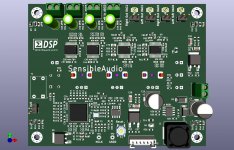
My current DSP:
So you have the programmer always connected and always on?
I2C?
Had any problems in this?
Sure phantom power would be able to fry it all up 😉
I2C?
Had any problems in this?
Sure phantom power would be able to fry it all up 😉
I'm not having much luck finding bi polar electrolytic caps a reasonable prices and availability here in the UK, something that may interest you though is UWP1V100MCL1GB nichicon bipoalar 10uF 35V smd available directly from JLCPCB.
USBi is powered by USB cable, SPI to DSP, does not matter whether I power up DSP before or after connecting USB cable from PC to USBI. So long as the same SS schematic is in the DSP and loaded on the PC then just link/ compile and can plug/unplug freely and will just work.So you have the programmer always connected and always on?
I2C?
Had any problems in this?
So you'll go with SPI for the programming?
I think I'll try to make a programmer based on the Cypress chip, just to verify it actually works before integrating it on a dsp board.
Cool with the UWP1V100MCL1GB
I think I'll try to make a programmer based on the Cypress chip, just to verify it actually works before integrating it on a dsp board.
Cool with the UWP1V100MCL1GB
Yes, as works for me on my current dsp.So you'll go with SPI for the programming?
I was going to integrate it but with it costing so much in extended part charges I will just buy the same board I'm currently using ready made from aliexpress, will work out a lot cheaper at approx €4 each.I think I'll try to make a programmer based on the Cypress chip, just to verify it actually works before integrating it on a dsp board.
- Home
- Source & Line
- Digital Line Level
- 4 in 8 out DSP using ADAU1652