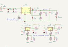
Just realize that AMS1117 is part of the basic components .... not sure it is better than LM317, but it is for sure smaller ....
Still wondering is I should include 3V3 zenners on the programming interface to protect from possible 5V interface input ..... wonder if the inputs on the DSP is actually already protected .. would make sense ...
Still wondering is I should include 3V3 zenners on the programming interface to protect from possible 5V interface input ..... wonder if the inputs on the DSP is actually already protected .. would make sense ...
I've chosen to pay for an extended part here, the LDL1117 is MLCC compatible and has a worst case drop out of 600mv, so should run cooler on a lower supply rail from the switching regulator. It's also got a decently low noise spec and is an STmicro part:Just realize that AMS1117 is part of the basic components .... not sure it is better than LM317, but it is for sure smaller ....
https://jlcpcb.com/partdetail/Stmicroelectronics-LDL1117S33R/C435835
Can't see that they are needed if using a cypress based chip as 3.3V out, especially if integrating it. If your bringing out the SPI/I2C lines for any random programmer, then probably a good call, will also help protect against ESD.Still wondering is I should include 3V3 zenners on the programming interface to protect from possible 5V interface input
Found a supply of Panasonic SU bi-polar EL caps that will do the job, will use those if the boards work but test with some polarised caps that I have in my parts bin 🙂
I really like KiCad, so powerful and learning more every day, but the BOM creation seems a bit more cumbersome than what I'm used to.
Ended up installing the "Fabrication Toolkit" via the Plugin And Content Manager.
Seems to do the trick as long as you include a field called LCSC Part # in the schematics part, which I have already done.
Checking the .csv file in Excel i a bit cumbersome as well ... make a copy and change file type to .txt then open it and go through the wizard to se the file in columns
😱 I'm at 122 usd for 2 assembled boards ...... will spend some time for a check more before committing this.
ADAU1452 at a whopping 18,5 USD
22 USD for extended components fee
ADAU1452 at a whopping 18,5 USD
22 USD for extended components fee
32 Mbit SPI E2PROM at Mouser for les than 1.5€ 👍
M95P32-IXMNT/E
https://www.mouser.dk/ProductDetail/STMicroelectronics/M95P32-IXMNT-E?qs=By6Nw2ByBD3xLRoMab161g==
Guess it would work fine ...
Wonder whether you'll need to write the whole EEPROM every time though?? ..... that would take a lot og time though
Otherwise 4 Mbit at 3.5€
M95M04-DRMN6TP
https://www.mouser.dk/ProductDetail/STMicroelectronics/M95M04-DRMN6TP?qs=wnTfsH77Xs47afrs3bIJjQ==
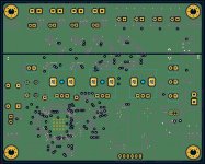
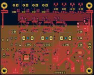
PCB sent of for production. Cost ca. 150 usd for 2 populated PCBs (few components will need to be hand soldered) ... so hope it works 😉
Attachments


Fingers crossed for you, I'm doing some final checks on my board now. I've decided to go with my existing ADAU1466 core boards, partly because the ADAU1466 'was' not in stock and all my SS files are for the ADAU1466, would take another load of work to redo them. Also if I've messed up, the cost would be higher, I have space on the PCB to modify for a version 2 and build everything onto the one PCB, will use this build to test all the Cypress, USB hub, Multiplex SPI switch, ESP32 interface plus DAC's and ADC's. If all working they will still be put to good use.PCB sent of for production. Cost ca. 150 usd for 2 populated PCBs (few components will need to be hand soldered) ... so hope it works
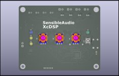
This is being built as a 4 x differential inputs +SPDIF (padded down and transformer isolated to accept AES/EBU input, 8 x impedance balanced outputs. USB hub for connecting Cypress and ESP32 and a multiplexer to switch the SPI control between the Cypress and the ESP32, plugging in a USB cable should auto switch to Cypress as SPI control.
With minor mods, this board can be configured to:
Inputs = 8x SE analogue in + 2 x SPDIF (10 channels in) OR 4 x differential inputs + SPDIF (current config)
Outputs = 4 x full differential outputs (@4VRMS) OR 8 (@2VRMS) impedance balanced (just don't connect '-' and becomes SE)
Edit, just to add that the I/O caps are bipolar 50V for 48V phantom power protection.
4 layer board, 5V analogue, 3.3V analogue, 3.3V digital, 5V digital for DSP and 5V auxiliary for ESP32 and Cypress all fed of the same switcher but using a 5.7V rail for LDO regs to reduce temperatures.
Ground plane is unbroken except for through hole components.
Attachments
Last edited:
For anybody thinking of using EASYEDA for a board of this complexity, it has become like surfing treacle, approx 15 seconds to add one just VIA 🙁
Why not to use this: https://jlcpcb.com/partdetail/AnalogDevices-ADAU1452WBCPZRL/C462188 ?ADAU1452 at a whopping 18,5 USD
22 USD for extended components fee
$3 less.
Not sure it was available when I did the component picking ... sure it would have been saving of 6 usd ...!
What do you mean ..... KiCad is running slow??For anybody thinking of using EASYEDA for a board of this complexity, it has become like surfing treacle, approx 15 seconds to add one just VIA 🙁
Don´t think EasyCad is made for this complex tasks ...
KiCad is running really well for me ... fast and really competent .... so if it takes 15 sec for a via I think something is wrong in your setup/installation!
Looking forward to hearing how it turns out, and hope you are willing to share schematics of especially for the Cypress part it it works .... will consider incorporating the programming interface next timeFingers crossed for you, I'm doing some final checks on my board now. I've decided to go with my existing ADAU1466 core boards, partly because the ADAU1466 'was' not in stock and all my SS files are for the ADAU1466, would take another load of work to redo them. Also if I've messed up, the cost would be higher, I have space on the PCB to modify for a version 2 and build everything onto the one PCB, will use this build to test all the Cypress, USB hub, Multiplex SPI switch, ESP32 interface plus DAC's and ADC's. If all working they will still be put to good use.
This is being built as a 4 x differential inputs +SPDIF (padded down and transformer isolated to accept AES/EBU input, 8 x impedance balanced outputs. USB hub for connecting Cypress and ESP32 and a multiplexer to switch the SPI control between the Cypress and the ESP32, plugging in a USB cable should auto switch to Cypress as SPI control.
With minor mods, this board can be configured to:
Inputs = 8x SE analogue in + 2 x SPDIF (10 channels in) OR 4 x differential inputs + SPDIF (current config)
Outputs = 4 x full differential outputs (@4VRMS) OR 8 (@2VRMS) impedance balanced (just don't connect '-' and becomes SE)
Edit, just to add that the I/O caps are bipolar 50V for 48V phantom power protection.
4 layer board, 5V analogue, 3.3V analogue, 3.3V digital, 5V digital for DSP and 5V auxiliary for ESP32 and Cypress all fed of the same switcher but using a 5.7V rail for LDO regs to reduce temperatures.
Ground plane is unbroken except for through hole components.
3, it is also extended.sure it would have been saving of 6 usd ...!
Cypress is aliexpress plugin module, already had a couple and trying to keep costs down. there are several schematics for the Cypress boards available online, just omit the unused lines. I was thinking of changing my build to a public share in EASYEDA, I think that would make it available to anyone wanting to play with the design but would like to check the PCB's are working first.Looking forward to hearing how it turns out, and hope you are willing to share schematics of especially for the Cypress part it it works .... will consider incorporating the programming interface next time
Got the PCBs back and have started testing.
I'm glad I had put in 2 0R resistors between regulators and the circuit, so I can make sure the voltage is ok before connecting it to the DSP circuit! Good practice 😉
A review more would have been in order, but of course I had not looked too much at the LM317 circuits, as how could this be wrong .... well guess again ... take a look ... result is 7 V instead of 3.3 😱
Well not so difficult to fix, but come on.
Also for some reason had ties the Enable on the switcher to GND, making it not start. Removing it, and it started and worked as expected 😉👍
Attachments
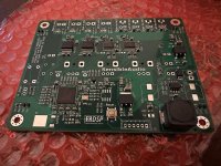
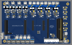
Ok. Have the board up and running.
All PSU voltages within spec
I can program it through I2C via my Wondom ICP3
I can flip an GPIO pin and light a LED
MCLK 24.5MHz
BLCK 3 MHz
LRCLK 48 kHz
I have no data out of the PCM1802 :|
I have not managed to send data out to the PCM5102A :|
Writing eeprom gives error when reading it back, and self boot does not work
Member
Joined 2018
Hello Baldin-San,
Now it's your turn on this issue.😱
Did you set up the hardware Config Tab?


Writing eeprom gives error when reading it back, and self boot does not work
Now it's your turn on this issue.😱
Did you set up the hardware Config Tab?
- Home
- Source & Line
- Digital Line Level
- 4 in 8 out DSP using ADAU1652