My suggestions:
1. Put about 10V zener diode between Q6 collector and V+VAS. Adjust R2 if neccessary. This will short collector AC voltage , which may othervise go to VAS input through Q6 Cbc.
2. And then connect Q37 collector to Q6 collector instead base, then adjust R22a if necessary. Usually Q37 start conduct at about 1/4 limiting value, so You must set limiting value very high, or risk some distortions.
Dear wojtek5001,
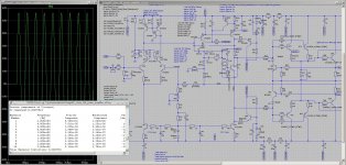
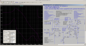
interesting idea. Please check the resulting schematic if I have correctly drawn your recommendations. Seems to work and overall distortion can be lowered as we can now use BC560C for Q6. It looks like the sticking bettered but this has to be verified in real life too. Think tuning D1 and R2 may bring here some interesting results. 🙂
BR, Toni
Attachments
Dear wojtek5001,
interesting idea. Please check the resulting schematic if I have correctly drawn your recommendations. Seems to work and overall distortion can be lowered as we can now use BC560C for Q6. It looks like the sticking bettered but this has to be verified in real life too. Think tuning D1 and R2 may bring here some interesting results. 🙂
BR, Toni
Very nice wojtek, Toni, thanks for this idea.
After doing some more simulation the new VAS protection and therefore the possibility to use BC560C instead of KSA992 brought some interesting results:
- As we now have better GM/PM I have retuned the TMC values: THD20k@200W@8R has decreased from 0.000454% to 0.000266% -
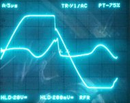
not very much but we take it as it is.🙂 - Sticking during overload has bettered significantly - see attached picture.🙂🙂
- PSRR+ 20Hz bettered from 88dB to 101db; 1kHz bettered from 116dB to 119dB; 20kHz bettered from 108 to 111dB
- PSRR- no changes: 20Hz 77dB; 1kHz 137dB; 20kHz 114db
Attachments
Last edited:
... wojtek's tip is working like a charm! Thanks for this tip!
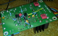
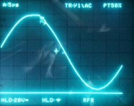
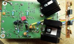
Attached my modified real life test sample and a quick THD20k test @50W@8R with very good results. The calculated TMC corresponds to real life. Square wave shows no ringing nor overshoot. Slewrate about 100V rising / 75V falling edge.
Sticking is a little bit better as before but already present.
Will redesign the Input/VAS pcb to reflect the changes - in 2014!
Happy new year to all DIY'ers!
Toni
Attachments
Last edited:
... real life test sample and a quick THD20k test @50W@8R
This photo is with the Cordell DM in place so the real result is 10x less than shown? Even .002% is fine, .0002% spectacular.
Happy New Year
David
This photo is with the Cordell DM in place so the real result is 10x less than shown? Even .002% is fine, .0002% spectacular.
Happy New Year
David
Thx.
I haven't used DM during this quick test. This will follow ...
Note: 0.002%@20kHz are hard to get with my analyzer testing only a wire.😉
Happy New Year
Toni
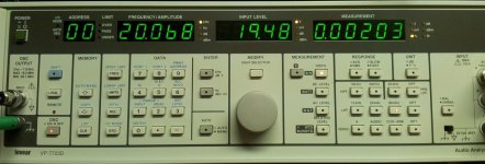
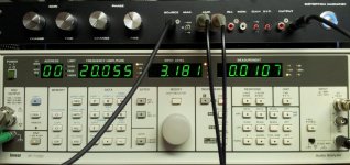
Now using DM:
THD+N20k@120W@8R
0.00107%@
THD+N20k@200W@8R
0.0012%
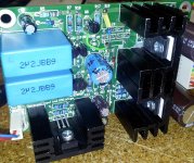
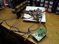
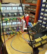
Better as all my results be4 VAS modification. Note: the test setup output stage has only 2 pairs of power transistors. So it is to be expected that the 8 pairs output stage brings us better results!
Attached some pictures of the test setup. Thanks again Bob Cordell for his really great tool - the "Distortion Magnifier".
THD+N20k@120W@8R
0.00107%@
THD+N20k@200W@8R
0.0012%
Better as all my results be4 VAS modification. Note: the test setup output stage has only 2 pairs of power transistors. So it is to be expected that the 8 pairs output stage brings us better results!
Attached some pictures of the test setup. Thanks again Bob Cordell for his really great tool - the "Distortion Magnifier".
Attachments

Now using DM:
THD+N20k@120W@8R
0.00107%@
THD+N20k@200W@8R
0.0012%
Better as all my results be4 VAS modification. Note: the test setup output stage has only 2 pairs of power transistors. So it is to be expected that the 8 pairs output stage brings us better results!
Attached some pictures of the test setup. Thanks again Bob Cordell for his really great tool - the "Distortion Magnifier".
Very nice test equipment you have, very good amp results.
All the best for New Year
Damir
Very nice test equipment you have, very good amp results.
All the best for New Year
Damir
Dear Damir,
thank you! Happy New Year and best wishes for 2014.
Toni
OT: discrete opamp / listening test
The first (subjective) listening test results at unity gain:
MyDOA v3 is neutral like a simple wire ...
... of course the other opamps tested bring the same results (NE5532, NE5534, LM4562, LME49990)...
BR, Toni
The first (subjective) listening test results at unity gain:
MyDOA v3 is neutral like a simple wire ...
... of course the other opamps tested bring the same results (NE5532, NE5534, LM4562, LME49990)...
BR, Toni
Attachments
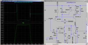
VAS current protection redesign: avoid overload / ringing
During redesign of vas protection I've made many real life overload tests to check the transistor and hence TMC modifications too.
A very small amount of overload @ 20kHz showed some ringing when the vas looses control. Was able to correct this problem with a little bit more compensation. NOTE: Could not simulate this behaviour.
I like the simulation tools very much but IMHO using the breadboard is minimum as important as simulation!
Attachments
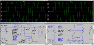
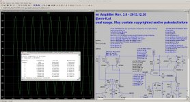
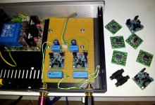
VAS current protection redesign: better sticking behaviour
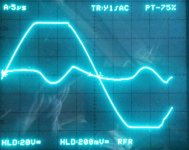
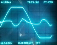
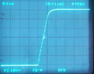
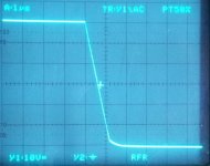
picture 1: baker clamp @ 1kHz + distortion residual
picture 2: baker clamp @20kHz + distortion residual
picture 3: diode clamp (D9 - see previous post), @20 kHz + distortion residual
picture 4: no clamp, @20 kHz + distortion residual
picture 5: test setup
load 8R resistive, analyzer bandwidth 80kHz.
The sticking behaviour at 1khz is for all variants the same - no sticking visible.
The next pcb will have a placeholder for D9 - using the diode clamp betters sticking but worsens 20kHz THD. So one can decide what is more important. The baker clamp doesn't help here very much in this configuration. Maybe there exists some better solution ...
Attachments

A note about the attached asc file:
KSC3503 and KSA1381 models are modified variants from Bob Cordells 2SC3503C and 2SA1381C: only BF has been adapted to reflect the current availability of these transistors: KSA1381E - hFe 130, KSC3503D - hFe 70.
KSC3503 and KSA1381 models are modified variants from Bob Cordells 2SC3503C and 2SA1381C: only BF has been adapted to reflect the current availability of these transistors: KSA1381E - hFe 130, KSC3503D - hFe 70.
Attachments
Toni, where is your Baker clamp?picture 1: baker clamp @ 1kHz + distortion residual
picture 2: baker clamp @20kHz + distortion residual
picture 3: diode clamp (D9 - see previous post), @20 kHz + distortion residual
picture 4: no clamp, @20 kHz + distortion residual
picture 5: test setup
load 8R resistive, analyzer bandwidth 80kHz.
50 V/us only and 20 kHz sticking from hundreds of parts per channel, not so impressive results don't you think? 😕
It's a work in progress. V3 isn't finished and maybe some measurements are not impressive. But even if this amplifier doesn't fit your personal component count upper limit and your personal V/µsec speed the THD and the current distortion spectrum is not so bad. (THD+N20k@200W@8R: < 0.002% measured using VP7723D; IMD 19k/20k@200W@8R < 0.002% measured using ARTA).50 V/us only and 20 kHz sticking from hundreds of parts per channel, not so impressive results don't you think? 😕
Stronger compensation wasn't done to prevent sticking at 20kHz. Only to find the reason for the oscillation bursts at overload using an 8R load. Removing the test load or increasing it to ~ 16R the oscillation bursts during 20kHz overload stop. Maybe my test setup is suboptimal (currently only 1/4 of the needed output power transistors are mounted, no ops pcb). The amplifier is stable using C1 = 47p which gives > 100V/µsec.
Simply need to find the reason for the overload bursts ... maybe someone can help here ...
Last edited:
- Home
- Amplifiers
- Solid State
- 2stageEF high performance class AB power amp / 200W8R / 400W4R