A regular soldering iron can be limited for powerpad, so grandma's flatiron in a linen mode and a paperclip will do the trick.It is 4x4 mm dust cooled by PCB, I wonder if a DIY can solder it with ordinary soldering iron.
H
HAYK
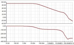
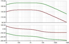
The precedent Bode plots are wrong. I have the habit to limit the frequency 100Mhz. Here the chip speaks up to 1Ghz. For the first time I switched to Ghz scale to measure audio amplifier.
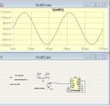
For unity gain the DS advises to use 510 ohms feedback resistor. I decreased it to 220 with a snubber and looks perfectly stable. I am simulating with the VAS stage to learn the behavior of the crossover. Bellow is the open loop 1W triangular output with 50ma bias.

I ordered 5pcs from Ali for about $5, I will learn how to solder without hot air although I have one.
For unity gain the DS advises to use 510 ohms feedback resistor. I decreased it to 220 with a snubber and looks perfectly stable. I am simulating with the VAS stage to learn the behavior of the crossover. Bellow is the open loop 1W triangular output with 50ma bias.
I ordered 5pcs from Ali for about $5, I will learn how to solder without hot air although I have one.
Attachments
Last edited by a moderator:

H
HAYK
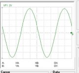
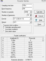
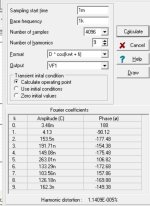
I adjusted the crossover for excellence. The 5th harmonic shows no any abnormal on the odd harmonics. On the other hand as I increased the votage/current ratio, the distortion is now 0.2% 1w@20khz. This will be the linearity of the internal impedance.
Attachments
H
HAYK
I am testing the VAS stage for best common base transistors.
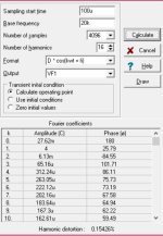
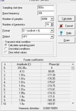
I closed the loop by unity gain buffer to imitate a perfect output,
The bd139 140 is very good in gain and distortion but to my surprise the 2n5401,5551 is the same with better frequency response. I tried what @minek uses A1381,C3503, desasterous.
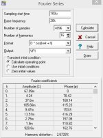
To note that the distortion measured 1w 20khz is 0.000036% but all the harmonics are equal, that is noise. With 22.5V, that is 30w it is 0.000012%.
I closed the loop by unity gain buffer to imitate a perfect output,
The bd139 140 is very good in gain and distortion but to my surprise the 2n5401,5551 is the same with better frequency response. I tried what @minek uses A1381,C3503, desasterous.
To note that the distortion measured 1w 20khz is 0.000036% but all the harmonics are equal, that is noise. With 22.5V, that is 30w it is 0.000012%.
Attachments

Last edited by a moderator:
H
HAYK
H
HAYK
Need help with ltspice.
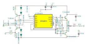
I have a working Tina model with opa2673 but gives a strange distortion impossible to decrease with feedback even 80db NFB. I switched to ltspice exactly the same circuit, it runs but measures nothing of the circuit. Why?
The opa model is not common, I made it auto-generated, the Pspice model is in the lib.
Attachments
You should include OPA2673 simbol and compo.lib.Need help with ltspice.
I have a working Tina model with opa2673 but gives a strange distortion impossible to decrease with feedback even 80db NFB. I switched to ltspice exactly the same circuit, it runs but measures nothing of the circuit. Why?
The opa model is not common, I made it auto-generated, the Pspice model is in the lib.
View attachment 1233113View attachment 1233115
H
HAYK
H
HAYK
H
HAYK
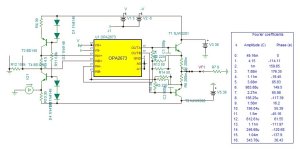
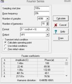
Now, this is something extraordinary. It is 100% current feedback that uses jfets as variable resistors to adjust the gain from 2x1 to 1x2 gradually by measuring the current. The bias current is only 5ma, even.
The distortion is 0.15% for1w20khz without any 5th harmonic over value but even order dominance because of mismatch of jfets which can be adjusted be the series 500 ohm resistors.
To note that this amp is open loop V/I converter.
If you need more explanation, the output is biased 5ma. Up to +/-10ma output it is classA with each pole adding its gain. When the output current exceeds 10ma one of the poles goes off and the gain is reduced from double to simple. Here the jfet controlled by the opposite poles current when it gets no voltage at cut off shorts the 500 resistor to double the gain of the active pole. As the jfet is a linear element by this it gradually increases the gain to get smooth passage from simple to double.
H
HAYK

H
HAYK
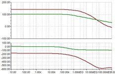
I tried the same circuit with ths6012, because of its higher gain, the distortion is nothing but 2nd harmonic which is due to k,j jefet mismatch that can be adjusted by R4,R5. The model of jfets is the V 16ma version which is no more available, more common are BL 10ma and GR 6ma.
What intriguing me is the mediocre response of the opa compared to THS which is supposed to be 3x higher GBW.

What intriguing me is the mediocre response of the opa compared to THS which is supposed to be 3x higher GBW.
Attachments
Last edited by a moderator:
H
HAYK
I closed the loop with 22k//1pF, the distortion is 0.0001% but only noise and this with ideal IPS,VAS. I can decrease the NFB by 60db to get it doubled. I am wondering if it does worth to go current mode. I will try the voltage mode using the opamps as buffers.
Attachments
H
HAYK
H
HAYK
H
HAYK
I replaced the output transistor with mjl3281/1302. Although the spec says the njw1302g 0302 are low power but more linear, the spice models says something else. With njw, I get 0.002% 1k 23Vpk but 0.02% with 20khz. With the replaced ones, I get 0.001 and 0.002%. What to believe.
I passed to LTspice with a working circuit. When I simulate in ac open loop with feedback inductor 1G and no input, it measures everything. As soon as I close the loop, it runs but measures nothing.
I passed to LTspice with a working circuit. When I simulate in ac open loop with feedback inductor 1G and no input, it measures everything. As soon as I close the loop, it runs but measures nothing.
Attachments
I never blindly trust spice models which are freely given by a vendor. They have enough fidelity to tell a system designer if something is basically going to WORK. Not to distinguish these teeny tiny differeneces in distortion. People pay money, big money to get models that DO. That business would evaporate overnight if it weren’t NEEDED in industry. My old college prof started one of those companies (Modelithics). It’s mostly RF devices, but the same idea.
There are any number of other reasons a larger “less linear” transistor simulates with lower distortion in a given circuit. You may just have a more optimum driver for the bigger part. It might not be dominated by hFE linearity. The way this circuit has evolved over the course of development it’s not even an “emitter follower” anymore - technically the output stage is common emitter. The signal is taken THROUGH the power supplies so it is deceptive. It just biases like a normal EF so it looks like one.
The 0302/0821 parts are physically smaller than their original counterparts, that’s ALL. Physically smaller die of the same construction can actually have the same SOA and hFE at full current. What that REALLY means is that the larger die was beyond the point of diminishing returns for those parameters. Making a transistor bigger does not always result in better if the additional die area isnt fully utilized. The current density inside these things is NOT uniform, otherwise there would be no such thing as second breakdown. Toshiba figured this out and ON followed suit. But the smaller die will ALWAYS have a lower capacitance and a lower AVERAGE temperature. Whether or not this trade is better depends on implementation.
And you’re modeling poles in the GHz? You ARE being led astray. Up there, unless the entire layout is being simulated (at least with dustributed transmission line models) you aren’t even CLOSE. Too many nanohenries off and those poles are going to move all over the place. And you’ll get a few more you weren’t counting on. Things above 50, 100 MHz generally don’t matter, but whe trying for this level of modeling fidelity they DO. They may or may not matter at all for SOUND QUALITY. I build stuff (work wise) in the GHz and without a layout model you are literally dead in the water. When design an audio amp (with stone knives and bear skins) I ignore anything above a few MHz because I know the model fidelity not to be good enough. Especially if I don’t have a PCB layout sitting right in front of me.
Oh yeah, and at this level, power supply models matter. It isn’t just a voltage source. And you are taking your signal THROUGH it. It’s a pretty good AC short, but there are more than a few nH in those big capacitors.
My whole point here is dont get hung up on .0000x % distortion at this level of simulation. You may or may not be able to do better with the tools you have. It’s inside of the numerical noise. That’s ok. Just BUILD something and see how it sounds, compared to other things you have bought/built.
H
HAYK
You are right, this is no more an EF, it is common emitter,. As I said on #56, all the extra components add to the first design doesn't pay in performance. The performance measured by simulator as I said is only a relative to see your design is better or worst.
Unlike tubes, SS are not precise component, the only thing that make them behave so is the feedback ratio. The higher you go in dB, the high you must go in frequency for stability. This is what unfortunate for audio amp design that one must spend most of the time for RF frequencies. By using the output as common emitters, the high frequency character of the drivers aren't of importance as with unity gain any of them whether 180Mhz or 600Mhz pole is the same in a chain limited by the pole of the output transistors which makes the circuit much easier to stabilize.
After working 10 days for enhancements without real success, I wanted to get something successful out of it and gave this result, simplicity. Physically, it is a tiny 70x30mm PCB with minimum components. May be I should have started a new thread after #56 with appropriate title with 1 stage output BJT instead of 1 EF.
- Home
- Amplifiers
- Solid State
- 1 EF AMP