Great, I will do it. Thanks@carcotado please move R33 + D2 and R32 + D3 to the left side of the T13-16.
As it is connected now, for example, think of 1 A current through R32 or R33 drawn via output transistors by the output load, theoretically it would cause a voltage fall of 47 Volts over these resistors (U = I x R), the voltage supply to the amplifier circuit will jerk terribly up and down with the audio signal.
I think you have made a mistake, first you said "then the P-Channel will be 594 ohm" and then "The nearest standard value is then 680 ohm for the N-Channel" same value for two channels, I think 680 and for channel N.If we pick say 470 ohm as a grid stopper for the N-channel, then the P-Channel will be 594 ohm. The nearest standard value is then 680 ohm for the N-Channel.
Thnks
carcotado, is this your own circuit? ie has an amp. to this circuit ever been built and tested to work well?
If there is no 'real life' working version of this, nearly all the suggestions here are just guesses which may or may not work as you've found.
The first step is to get your circuit close to something that is known to work properly. Then those who have real life experience of that circuit can tell you what to do if something is not right.
There are several icky points in your design but I'll just mention 2 which others have also pointed out
Have you simulated this in LTspice?
If there is no 'real life' working version of this, nearly all the suggestions here are just guesses which may or may not work as you've found.
The first step is to get your circuit close to something that is known to work properly. Then those who have real life experience of that circuit can tell you what to do if something is not right.
There are several icky points in your design but I'll just mention 2 which others have also pointed out
- Why are you using T3 & 4 as current mirror ?
- Why are you doubling up T8/9 & T10/11?
Have you simulated this in LTspice?

I echo @kgrlee's questions... Is this working design that others have built (with the same PCB layout) with success? Or are these PCB's you found somewhere without any evidence that they are proven to be functional?
The question is not to belittle or scold you... it simply helps us determine if we are troubleshooting a working design or if we are essentially prototyping a new design.
If it is a working design, having the original BOM from the source would help. Sometimes parts substitutions (for example to address obsolesce) can have detrimental effects.
Hi, as I said in the first post, this schematic is mounted and works well, but with Hitachi Mosfet 2SJ50 and 2sk135, I was looking for these mosfet, and I did not find them, so I bought Exicon as a replacement. Since then I am looking for a solution before discarding the project and losing the money.carcotado, is this your own circuit? ie has an amp. to this circuit ever been built and tested to work well?
If there is no 'real life' working version of this, nearly all the suggestions here are just guesses which may or may not work as you've found.
The first step is to get your circuit close to something that is known to work properly. Then those who have real life experience of that circuit can tell you what to do if something is not right.
There are several icky points in your design but I'll just mention 2 which others have also pointed out
Sorting these things out may not cure your problem but at least we will be on a known path instead of moving blind into the unknown.
- Why are you using T3 & 4 as current mirror ?
- Why are you doubling up T8/9 & T10/11?
Have you simulated this in LTspice?
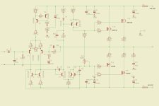
This is the original schematic.
I haven´t silulate it in LTspice.
I think with the 470 and 680 Ohm gate resistors, it goes well. I show oscilloscope measurement video. In test with music, it sounds good and no abnormal noises can be heard.
Thanks
Attachments
The gate resistor doesn’t matter. You should look at other stuffs more important.I think with the 470 and 680 Ohm gate resistors, it goes well.
C8 is suspiciously high value. I don’t think the schematic is the original. Please link the original schematic. If it is the original, then I can say it is poorly designed.
The Crown Pulse topology is verry prone to oscilation, I started audio with their design and had alot of hard time. Their design hass verry good bass, the speaker barely moves and brings the house design. The VAS stage is replicating a simetrical amplifier because of using signal from both transistors in input stage. Later Edit: Below are some pictures of a factory design with Mosfet from General Music Italy.
Attachments

Last edited:
Hi, as I said in the first post, this schematic is mounted and works well, but with Hitachi Mosfet 2SJ50 and 2sk135, I was looking for these mosfet, and I did not find them, so I bought Exicon as a replacement. Since then I am looking for a solution before discarding the project and losing the money.
This is the original schematic.
Is the PCB you are using a proven implementation of this design?
Sorry, I don't have the link, this schematic was given to me by a friend who assembled this amplifier and it worked fine for him.The gate resistor doesn’t matter. You should look at other stuffs more important.
C8 is suspiciously high value. I don’t think the schematic is the original. Please link the original schematic. If it is the original, then I can say it is poorly designed.
Because C8 is too high, what should it be?
Thanks
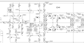
No, PCB is designed for me. Would you like to see it?Is the PCB you are using a proven implementation of this design?
Do I have this right; You have a friend using the same PCBs and same schematic and it is working for him. Is the only change from his build you are aware of the switch to Exicon Lateral Mosfets?
EDIT: I saw you previous post. Are these the same or different PCBs?
EDIT: I saw you previous post. Are these the same or different PCBs?
Yes, it is the same schematic, the PCBs are not the same. Components the only change were the EXICON, and it was not working, now I have changed some component like the Miller capacitors, something else you see in post #49, which has improved over the original.Do I have this right; You have a friend using the same PCBs and same schematic and it is working for him. Is the only change from his build you are aware of the switch to Exicon Lateral Mosfets?
DifferentI saw you previous post. Are these the same or different PCBs?
@carcotado can you tell what type of resistors (R25-28) are used as Source resistor for the power FET's?

If these are wire wound resistors, especially Lateral FET's can easily run into oscillation because of the relatively high inherent inductance in the these types of resistors, in that case it doesn't matter much what value the compensation capacitor has (C8), or the gate resistors are, because the oscillation will be local around the FET itself, in particular the N channel FET is prone to run into oscillation bursts at the positive peak, or just a bit after the positive peak when the signal starts to slope downwards, which can be observed using a sinus test signal.
So, if these resistors are wire wound then these must be changed to film type resistors.
There have been few suggestion to move the FET gate resistors (R21-24) as close as possible to the FET gates, which I also think is quite important, I went through the whole thread but can not see any reply from you in this matter, did you try this modification or not, and what was the result?
Also, the way the PCB gate drive traces are designed is not properly done, there should be no large areal traces at all, quite the contrary the traces should be as slim as possible, 1 millimeter wide traces is well enough for gate driving.
Rerouting compensation capacitor C8 was also mentioned, i.e. connect the side of C8 that goes to output instead to the VAS stage, the collectors of T10-11, collectors of T8-9 may also work.
It's also not very clear from your posts how many combined modification you have tried out concurrently, however, it is often necessary to try several combinations at the same time before one can see a working effect, that could mean trying following three modifications concurrently;
1. Connect gate resistors physically close to FET transistor, max couple of millimeters from FET gates.
2. Reroute C8, i.e. move one leg from output instead to VAS stage.
3. If the source resistor R25-28 are wire wound, then changed them to film type resistors.
Another question mark is the PCB layout design, but I didn't look too carefully for now.
OK,I will compare it with the other PCBIf the design is working with a different layout, then my suspicion is that your issue is layout related, not the switch to Exicon devices. The troubleshooting setup others have recommended are likely simply mitigating a layout issue.
and put nothing?I can see #49 is getting somewhere stable.
You could remove C8.
Yes they are Wirewound Resistors (pdf)If these are wire wound resistors, especially Lateral FET's can easily run into oscillation because of the relatively high inherent inductance in the these types of resistors, in that case it doesn't matter much what value the compensation capacitor has (C8), or the gate resistors are, because the oscillation will be local around the FET itself, in particular the N channel FET is prone to run into oscillation bursts at the positive peak, or just a bit after the positive peak when the signal starts to slope downwards, which can be observed using a sinus test signal.
So, if these resistors are wire wound then these must be changed to film type resistors.
I did it, I didn't notice anything substantial, now are mounted near. the tracks somewhere are thicker.There have been few suggestion to move the FET gate resistors (R21-24) as close as possible to the FET gates, which I also think is quite important, I went through the whole thread but can not see any reply from you in this matter, did you try this modification or not, and what was the result?
Also, the way the PCB gate drive traces are designed is not properly done, there should be no large areal traces at all, quite the contrary the traces should be as slim as possible, 1 millimeter wide traces is well enough for gate driving
is referred to as shown in the image?Rerouting compensation capacitor C8 was also mentioned, i.e. connect the side of C8 that goes to output instead to the VAS stage, the collectors of T10-11, collectors of T8-9 may also work.
Attachments
After reading this lengthy thread, it's clear that the 8-9 MHz oscillation means it's an output stage problem. Here are my suggestions:
1. If you have that diode+47R series combination in the supply rails, bypass it to take it out of the circuit.
2. Put high frequency decoupling of each output transistor with 100nF to ground as close as possible to each drain terminal.
There is very little HF decoupling in the schematic.
3. Try increasing the gate stoppers to a high value, say 680R each and note the effect.
Does it reduce or eliminate the oscillation?
If it eliminates it, then you can gradually reduce their value to the point where it starts to oscillate, then increase again to the next stable value.
4. If it reduces oscillation but doesn't eliminate it, then I would try some non-inductive emitter resistors, such as metal element current sense resistors.
Adding to @kapitiaudio steps, you might also consider removing/disconnecting one of the output pairs and resetting the bias. Then check for stability. This would let you know if the issue is due to paralleling OPS devices or something else.
- Home
- Amplifiers
- Solid State
- Help with an oscillating amplifier with Exicon mosFET ECF10P20 & ECF10N20