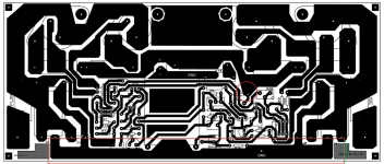
I took a look at the layout from post #29. Two quick observations:
1) The NFB takeoff point is probably fighting with the output currents. I would suggest routing it off of a T junction near the output connector. There are quite a few threads on this forum describing how this should ideally look. I tried to draw in an example of how it might look. Currents are low so the trace can be thin.
2) The grounding layout may be injecting charging pulses from C11/12 into the input. Ideally, the grounds for the two main caps (C11 & C12) should join together first, then this union should flow into the remaining ground points. The way you have it, the input is in the path of the returns for C11 & C12.
Attachments

Please ask your friend where he got the circuit from and if there are any measurements of the original circuit by the designer. The circuit is so badly designed that it is likely some faults have cancelled out other faults.Hi, as I said in the first post, this schematic is mounted and works well, but with Hitachi Mosfet 2SJ50 and 2sk135, ... This is the original schematic.
The EXACT PCB layout also influences whether this happens or not.
If you are happy with this, I think you should stop and be happy. Has the 'sputtering' you mention in #49 gone?I think with the 470 and 680 Ohm gate resistors, it goes well. I show oscilloscope measurement video. In test with music, it sounds good and no abnormal noises can be heard.
But be careful if you change your speakers as a different load could re-introduce the oscillation.
Last edited:
Reading this made me think.If you are happy with this, I think you should stop and be happy. Has the 'sputtering' you mention in #49 gone?
But be careful if you change your speakers as a different load could re-introduce the oscillation.
Yes, the the sputtering has gone. I will check with other speakers as well.
I am going to make a summary because I don't think I have explained myself well.
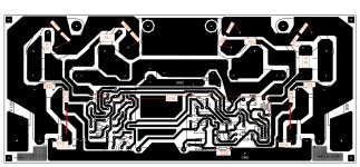
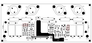
The first problems are the ones described in post 1 and following. After your advice, readings and tests, I arrive to the scheme of post #49, in which I find the problem of sputtering, which was solved by increasing as you told me the gate resistors to 470 and 680 Ohm. and this is the board as I have arranged the components. Capa Top y Botton. (In red the modifications in the track layer, with some bridge and wired track).
Now, it does not make noise in vacuum, Bias measurements remain stable around 10mV, Offset between 3 to 5 mV.
Only in the video, it reproduces the moment in which I have injected a 1 KHz signal with the level shown (red signal) and I turn on the amplifier and the output signal (blue), it moves a little and I don't know if it is ok or not. As I said my knowledge in this field is not very big and I keep learning with your advice.
In listening tests, I think it sounds good, but as I say it is my first project and my knowledge is not great.
I am enormously grateful for your advice and learning, but at this point I say the above, because in the absence of knowing if the signal measurement on the oscilloscope is OK, I do not see something wrong (from my little knowledge),
Bias stable,
Offset, within the range (I would like it to be 0, but I do not know how)
Also I do not know if there is another measure to do?
Thank so much
Attachments
Do you really have 47R resistors placed before the output devices? These will drop an enormous amount of voltage as soon and you push any power through it. They will probably fry unless they have a very high power rating.
Typically, if these are used, they are placed after the output devices where the current levels result in less voltage drop. They form a low-pass RC filter with C9/C10 to improve PSRR.

Typically, if these are used, they are placed after the output devices where the current levels result in less voltage drop. They form a low-pass RC filter with C9/C10 to improve PSRR.