Yes, in the new schematic it´s 180pF, both. C6, C7If you increase that C the self-oscillations will disappear
Yes, This is how is mounted.This should work, but they must be very close to the gates. Several cm of track or wire to the stopper is enough to turn the lateral into a radio transmitter
I seet, but I would like to get my design working before trying a new designThe source connection of the MOSFET needs protection from capacitive loads. The small inductance of a wire-wound resistor as shown can provide this, a 0R22 value will do more than 0R1 in that regard. The gate stopper resistors will do better if there is a low pass filter capacitor between the gate and the source. The gate stopper resistors could be increased in value up to 330R and the capacitor value introduced between gate and source, decided by trial and error. This circuit looks tidier for stability as there is only one capacitor around Q4 however the value might need to be changed. This could be connected from the collector of Q4 to the base of Q2 as has been indicated in another input suggestion. I would not recommend a lead capacitor in parallel with the feedback resistor as any hf instability due to the load will be introduced to the system

Check the
Revisiting lateral MOSFET stability
The ceramic insulators work because internal reactances no longer couple capacitively to the heat sink. The gate to drain capacitors enhance the gate stoppers because they bypass internal reactances. Also, bypass all drain connections to a heavy ground conductor with .47 uF or larger film cap. There are some disagreements in the replies, but at the end of the day, this is working in production amplifiers for us.Thanks, but my question is about post #49, in which I use Exicon ECF Mosfet, TO3Try 470 ohm gate stopper on the 2SJ162 and 680 ohm on the 2SK1058.
"Transistorlegacy,
Check theThe ceramic insulators work because internal reactances no longer couple capacitively to the heat sink. The gate to drain capacitors enhance the gate stoppers because they bypass internal reactances. Also, bypass all drain connections to a heavy ground conductor with .47 uF or larger film cap. There are some disagreements in the replies, but at the end of the day, this is working in production amplifiers for us."
I have read the link, in this case, I understand that this is for plastic Exicom Mosfet, and in my case I use Exicon Mosfet with TO3 metal encapsulation.
Sorry, I realized that in the schematic I put D2 wrong, so I think, ¿It is the same as you tell me?D3 is backwards, C4 should be Nichicon UES bipolar type - 220 to 470 uf / 25/35 volts - bigger uf is better and higher voltage is better
Attachments
YesExicon MOSFETs have the same capacitances as the older Hitachi parts. See data sheet.
I have seen this, but, because most of the schemes with HITACHI mosfet, have gate stop resistor of the same value? I have only seen it in Exicon, have a different value. And, in this case 470 and 680, could it reduce the slew rate?
Also, different values produce different Bias measurements on the source resistors, as I said, how does this affect?
Thank so much.
The slewrate is really driven by the driver stage current. Typically 10mA for these MOSFETs. The grid stopper is not big enough to make a huge difference here. But they do stop oscillation. Some designs have used 1K here. Some 470 ohm (see HAFLER 200). But looking at the EXCION data sheets, we see that the the Ciss is not the same:

Coss is the same. And Crss is very small. If we add them together for a source follower application, we get:
N-Channel: 810pF
P-Channel: 1025pF
So the ratio between the two is 1.27
If we pick say 470 ohm as a grid stopper for the N-channel, then the P-Channel will be 594 ohm. The nearest standard value is then 680 ohm for the N-Channel.
You can experiment with lower values, - but I doubt you will be able to hear any difference. The key here is to make the stoppers large enough to avoid parasitic oscillation. You can also go bigger: 1K - 820ohm. Or lower 470 ohm - 390 ohm. You get the point... 🙂
ok, thanks for your answer, I understood the reasoning. I will do it with these values.Coss is the same. And Crss is very small. If we add them together for a source follower application, we get:
N-Channel: 810pF
P-Channel: 1025pF
So the ratio between the two is 1.27
If we pick say 470 ohm as a grid stopper for the N-channel, then the P-Channel will be 594 ohm. The nearest standard value is then 680 ohm for the N-Channel.
You can experiment with lower values, - but I doubt you will be able to hear any difference. The key here is to make the stoppers large enough to avoid parasitic oscillation. You can also go bigger: 1K - 820ohm. Or lower 470 ohm - 390 ohm. You get the point... 🙂
Another question, why do we do it "add them up for a source follower application"?
Where can I read more about this, to understand it better?
Thank so much.
... But looking at the EXCION data sheets, we see that the the Ciss is not the same..
Where did you find this? In the the current datasheets on Profusions site for the single die devices, each channel in its own sheet. And the N channel and P-Channel show the exact same capacitances. Which does not seem correct. Further, the chart of capacitances is only in the P-Channel datasheet and this chart does always tie to the stated values. You can take a look for yourself here.
Its a similar situation for the double die devices. The chart only exists on the P-Channel and it doesn't seem to tie to the datasheet values.
I've sent an email into Profusion to ask about this. Haven't heard back yet.
For example, this is from the ecx10p20 datasheet. The table is the exact same values as the ecx10n20 which does not seem right.
- Ciss: 500 stated for Vgs=0V Vds=10V. The chart shows 500. Looks OK.
- Coss: 300 stated for Vgs=0V Vds=10V. The chart shows 390. Does not tie.
- Crss: 10 stated for Vgs=0V Vds=10V. The chart shows 10. Looks OK.
And this is from the double Die P-Channel: https://www.exicon.info/PDFs/ecw20p20.pdf
- Ciss: 1850 stated for Vgs=0V Vds=10V. The chart shows 950. Does not tie.
- Coss: 850 stated for Vgs=0V Vds=10V. The chart shows 725. Does not tie.
- Crss: 55 stated for Vgs=0V Vds=10V. The chart shows 30. Does not tie.
Am I looking at this right? Is this confusing to anyone else?
Everything I have read on Lateral MOSFETs says to focus on the input capacitance and the pole created by it and the gate stoppers. Using different gate resistors values between N and P channels accounts for this. I can see this in simulations when assessing slew rates. I get very asymmetric behavior if the resistors are the same value.
Having said this, there are several successful designs that use a single value (Mooly's amp for example).
Having said this, there are several successful designs that use a single value (Mooly's amp for example).
1. The necessity of the stopper resistor is exaggerated. Some official document of other MOSFETs only use 25 Ohm as the stopper to spec rise time. Using something bigger than 100 Ohm is just waste of performance.
2. To be more specific, for common vertical MOSFET, you only need to care the Crss. The reason is that the input capacitance is bootstrapped by the source follower. The input capacitance doesn't matter. The Lateral MOSFET is more complicated. It has lower gm. The voltage gain of the output stage is about 0.9 in practical. Thus, the total capacitance is about (1/10*Ciss) + Crss. In general, the effect of the input capacitance is way smaller than you think.
2. To be more specific, for common vertical MOSFET, you only need to care the Crss. The reason is that the input capacitance is bootstrapped by the source follower. The input capacitance doesn't matter. The Lateral MOSFET is more complicated. It has lower gm. The voltage gain of the output stage is about 0.9 in practical. Thus, the total capacitance is about (1/10*Ciss) + Crss. In general, the effect of the input capacitance is way smaller than you think.
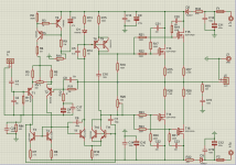
@carcotado please move R33 + D2 and R32 + D3 to the left side of the T13-16.
As it is connected now, for example, think of 1 A current through R32 or R33 drawn via output transistors by the output load, theoretically it would cause a voltage fall of 47 Volts over these resistors (U = I x R), the voltage supply to the amplifier circuit will jerk terribly up and down with the audio signal.

As it is connected now, for example, think of 1 A current through R32 or R33 drawn via output transistors by the output load, theoretically it would cause a voltage fall of 47 Volts over these resistors (U = I x R), the voltage supply to the amplifier circuit will jerk terribly up and down with the audio signal.
- Home
- Amplifiers
- Solid State
- Help with an oscillating amplifier with Exicon mosFET ECF10P20 & ECF10N20