Thanks Rayma, I have watched a thousand videos, I have finally found a way that seems to work for so small parts. But I would prefer 1000 times to get them soldered from JLPCB. Currently, I recreate all my PCBs in SMD. Last control I created has 130 components and needed 3 hours to solder each board, so SMD will be solution...
I have even more ideas . A FET where the pos and neg temp coefficient cancel at lowerI'd propose Miraculix for a really fast PNP. Maybe SiGe. Would not need to be really low cost. There is no competition. The mass extinction of RF PNPs starts to limit design choices such as active pull ups or folded cascodes.
Or a LMH6702 or the "newer version on steroids" with a JFET buffer in front. Sometimes
a CFB is nice but the input current hurts.
currents. I have a FET amplifier where there is no feedback around the FET input stage.
Thus, I must rely on TC canceling to get stable gain over temperature. I happened to hit
the sweet spot with 16 * CPH3910 at 45 mA total or so. No gain deviation worth speaking
of between between 20 and 60°C and beyond. With the JFE150, I get 7 dB variation from
20 to 60°C. The gain stability sweet spot seems to be at 6 JFE150s at the given 45 mA.
That impairs my voltage noise spec. All from Spice / ADS simulations. OK , I have
measured the 16*3910; their voltage noise is somewhat worse than the simulation, and
their spice model has no 1/f.
I also would be interested in a super-beta BJT that deserves its name. Say beta = 2k.
Early voltage does not matter, we know cascodes. 3V VCE_NOT_OPEN_BASE is OK.
I'm just digging into Bob Widlars voltage follower that seems to have surprisingly low
voltage noise, according to simulations using BJTs with Vbe == Vce, ie. 07V for both
with bootstrapping. You seldom see voltage gain = 1.000 on a follower.
2SD2704 seems to be one of the very few discrete SuperBeta transistors available.
And it is a lowly switch.
I know that Bob Widlar offends / scares JFET people. 🙂
Having an extra-low-noise Widlar voltage follower could remove the input current
burden from an array of OpAmps or BJTs as the voltage gain stage.
I know, this is against the notion that the input stage should have as much voltage
gain as possible. But, as Cesar said: divide et impera!
Cheers, Gerhard
Where do you propose to obtain a discrete "charge storage PNP" like the one Widlar used in his LT1010 voltage follower ?
_
_
Attachments
Ah, Bob Widlar wasn't a one trick pony 🙂
I'm thinking at the input stage of his BJT Ersatz-JFET opamp.
Don't hit me for this circuit, I'm still stumbling around.
I can prove everything and the contrary.
More input transistors seem not to drive the noise further down,
more current does. With just 3 cent-transistors, 400 pV/rtHz
looks respectable, and that with low input current.
Q1 and Q2 have 0.7Vdc for Vbe AND Vce.
Attachments
Last edited:
I also would be interested in a super-beta BJT that deserves its name. Say beta = 2k.
Early voltage does not matter, we know cascodes. 3V VCE_NOT_OPEN_BASE is OK.
2SC3624
Attachments
Oh, it seems it's dead. Digikey still has some but not via web site ordering.
You've got to call, probably they want to sell all they have in one order.
You've got to call, probably they want to sell all they have in one order.

Yes, this is correct. Actually the data sheet should say 4 kOhm; ideally you want to increase the JFET gain stage as much as possible without getting close to the linear region. 4 kOhm gives ~ 8V drop, leaving ~ 3.3 V across the drain-to-source. I'll fix on the next revision, thank you for the catch.Yes, the schematic is wrong. With Rs=300ohm and the typical Idss=35mA, the drain current is around 3mA. Therefore, to have the JFET in saturation Vds>Vgs-Vt, the drain resistor Rd should not be larger than about 3kohm, 10kohm is not good for a 12V supply. Probably a typo, Rd should be 1kohm.
Another note on that resistor; the input stage gain will help ensure low-noise operation, and allow for use of a lower Iq/higher noise OPA. But keep in mind the current noise of the amplifier will multiply with this impedance, which will become a substantial noise contributor if you attempt to use an amplifier with high IB, which is why we selected OPA202.
Hi Alexopth,At last some results on the phono stage, after almost two months I have only used JFE150 for the implementation, no other active device. So:
- SC70 gave me nightmare to solder. Besides that, I didn't know if some issues I had were because of bad soldering. After a lot of experiments I learnt how to solder them but still I have doubts. WHEN LCSC is going to have them so they can solder for me?? PLEASE
- It is 1st time that I had such a difference from simulation to reality, more than 30% and because my circuit is very sensitive, it gave me too much trouble to experiment on the bench.... I managed to reach to a point where voltages are the same in two channels but resistor values are very different. However I checked every connection 10 times to ensure good soldering of everything.
- Sound seems very promising, it was compared to a Symphonic Line phono stage, for now I have stability issues with psu.
Thanks for the feedback!
Sorry about the difficulty soldering, but, it hopefully saved some board space 🙂?
Can you elaborate more on the difference between simulation to reality - what was the configuration? There will be device variation, of course, but 30% difference from simulation to bench is more than I would have expected.
Mike
Gerhard,I have even more ideas . A FET where the pos and neg temp coefficient cancel at lower
currents. I have a FET amplifier where there is no feedback around the FET input stage.
Thus, I must rely on TC canceling to get stable gain over temperature. I happened to hit
the sweet spot with 16 * CPH3910 at 45 mA total or so. No gain deviation worth speaking
of between between 20 and 60°C and beyond. With the JFE150, I get 7 dB variation from
20 to 60°C. The gain stability sweet spot seems to be at 6 JFE150s at the given 45 mA.
That impairs my voltage noise spec. All from Spice / ADS simulations. OK , I have
measured the 16*3910; their voltage noise is somewhat worse than the simulation, and
their spice model has no 1/f.
I also would be interested in a super-beta BJT that deserves its name. Say beta = 2k.
Early voltage does not matter, we know cascodes. 3V VCE_NOT_OPEN_BASE is OK.
I'm just digging into Bob Widlars voltage follower that seems to have surprisingly low
voltage noise, according to simulations using BJTs with Vbe == Vce, ie. 07V for both
with bootstrapping. You seldom see voltage gain = 1.000 on a follower.
2SD2704 seems to be one of the very few discrete SuperBeta transistors available.
And it is a lowly switch.
I know that Bob Widlar offends / scares JFET people. 🙂
Having an extra-low-noise Widlar voltage follower could remove the input current
burden from an array of OpAmps or BJTs as the voltage gain stage.
I know, this is against the notion that the input stage should have as much voltage
gain as possible. But, as Cesar said: divide et impera!
Cheers, Gerhard
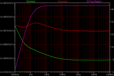
Good info. here, thank you. Are you saying you achieved zero TC with 6x JFE150 at a total of 45 mA?
I would have expected the zero TC current just greater than 10 mA:
Note on JFE2140, it is a smaller area device, the zero TC is achieved at a lower ID:
Regarding the follower, we do see it in many circuits that don't need ultra-low noise performance, it is easier to deal with but of course the noise adds directly without the benefit of a gain division. I don't know exactly what the Widlar voltage follower is; can you give a link?
Thanks,
Mike
< https://sci-hub.yncjkj.com/10.1109/jssc.1969.1049994 >
Fig 10. The pic is somehow mirrored.
At least it were 6 in the simulation of my circuit. I decided to wait for
real hardware to check this out.
Fig 10. The pic is somehow mirrored.
At least it were 6 in the simulation of my circuit. I decided to wait for
real hardware to check this out.
Hi Alexopth,
Thanks for the feedback!
Sorry about the difficulty soldering, but, it hopefully saved some board space 🙂?
Can you elaborate more on the difference between simulation to reality - what was the configuration? There will be device variation, of course, but 30% difference from simulation to bench is more than I would have expected.
Mike
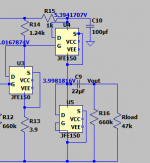
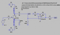
yes, check circuit below fed with 28V. The voltages are the ones on the real circuit but:
- R13 is 10 Ohm
- R15 is 780 Ohm
On the 2nd channel to have same voltages R15 is 900 Ohm.
I dunno maybe my soldering is not the best and contacts have issues but today the phono stage was on the system. I don't have distortion analyzers etc, only music matters to me. So first impressions are excellent but it seems I have to adjust the RIAA curve a little. Impressive detail.
Attachments
Update (please send to LCSC so we can have pre soldered boards)
I manage now to solder them correctly with simple iron. Destroyed a dozen before I learn how to do it.
I received 25 more from mouser to play.
News from the phono stage:
-It proved out that my circuit is very sensitive to resistance variations, that's why I got such differences. 1st stage I use 2 JFETs in parallel and follows exactly the simulation, interesting.
I have problems in other design with PJFETS, they are so scarce these days, any chance you produce PJFETs?
I manage now to solder them correctly with simple iron. Destroyed a dozen before I learn how to do it.
I received 25 more from mouser to play.
News from the phono stage:
-It proved out that my circuit is very sensitive to resistance variations, that's why I got such differences. 1st stage I use 2 JFETs in parallel and follows exactly the simulation, interesting.
- It takes half an hour to stabilize due to thermal I guess.
- They seem to produce the best sound when are near the 20mA in final stage
I have problems in other design with PJFETS, they are so scarce these days, any chance you produce PJFETs?
Hello.
I have a potential use for a pair of the TI JFE2140 in the esteemed Yamaha A-1 amplifier. And maybe also the C4 preamplifier.
They both use the 2SK100, now unobtainable. I can source and use the 2SK109 which apparently works but is not very low noise?
My questions:
Would the JFE2140 likely perform better?
If so, how would this present in terms of better SQ?
Is there in existence a pcb/adapter/workaround technique to help fit this SMD to the board?
Any advice appreciated.
Many thanks.
Does anyone know how to connect power to JFE150 JFET? Do you simply connect a 40v/-40v rails to VCH and VCL like it’s a op-amp? I want to use it in place of a J201.
JFE150 noise testing setup -- per the datasheet -- the one issue I am having is deriving a very low noise bipolar source ~50V (batteries and cap multiplier perhaps?). One issue with the 3,000 uF electrolytic on the Source -- noise in large electrolytic capacitors:
Attachments
The Art Of Electronics 3rd Ed. shows their schematics for their noise test fixture. BJT cap multiplier with ladder filter to the base is part of the supply network.
For apples-to-apples comparison, Vds is kept constant at 5V, the gate grounded and V+, V- adjusted for the current specified. So to compare a matched pair of BF862, CPH3910 to a JFE2140 I would like to follow their procedure.
Cap multiplier with adjustable voltage references a la AoE3
Cap multiplier with adjustable voltage references a la AoE3
Attachments
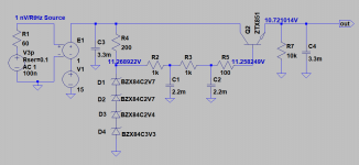
While one might want to compromise with lower voltages, and lower Rd and Rs (well, Rs is essentially shunted to ground), the noise contribution of Rd is inversely related to its value...no free lunch.
- Home
- Vendor's Bazaar
- Ultra Low Noise JFETs from Texas Instruments