I think that the values of Rd and Rs in the circuit shown in Figure 9-6 of the datasheet won't work.
Yes, the schematic is wrong. With Rs=300ohm and the typical Idss=35mA, the drain current is around 3mA. Therefore, to have the JFET in saturation Vds>Vgs-Vt, the drain resistor Rd should not be larger than about 3kohm, 10kohm is not good for a 12V supply. Probably a typo, Rd should be 1kohm.
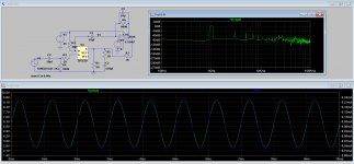
We have feedback so things are a little different but it works at about 1mA, here are results.
P.S. input should be below 10mV

P.S. input should be below 10mV
Last edited:
There's not really any sort of technology barrier to us making discretes, rather the question for all semiconductor companies is what is the profit generated per wafer? In many cases the discrete business has been "commoditized" to the point where the profit per wafer is extremely low, and it makes more sense to build other products using that capacity in your factory. High performance JFETs just happen to be one area where two well-matched transistors actually garner a higher price than with the rest of the op amp we usually put around them... 😉
The process technology used for the JFE150/2140 is the same bipolar process we use for op amps such as the OPAx140/164x/827/828/145 among many others.
I can see a manufacturer building high-performance opamps, and take the wafers that fail some opamp test, and laser-disconnect the opamp part and sell the remaining input pair as a matched pair to save the day.
Win-win for all!
Jan
We have feedback so things are a little different but it works at about 1mA, here are results.
P.S. input should be below 10mV
View attachment 998572
Check the Vds, your simulation shows the JFET is barely in saturation. Or it could be the device model doesn’t use the typical parameters from the data sheet (Vt=1.2V, Idss=35mA).
Last edited:
I can see a manufacturer building high-performance opamps, and take the wafers that fail some opamp test, and laser-disconnect the opamp part and sell the remaining input pair as a matched pair to save the day.
Win-win for all!
Jan
That is a very good idea, but maybe the reason why the opamps fail the test is because of the missmatch of the input pair?
Just a thougt.
Stein
Check the Vds, your simulation shows the JFET is barely in saturation. Or it could be the device model doesn’t use the typical parameters from the data sheet (Vt=1.2V, Idss=35mA).
Correct it is not in saturation at all but I have seen implementations (and I have made tests myself) with JFETs not in saturation area. There is a circlotron design only with JFETs that the input stage works with JFETs not in saturation area (linear ?)
The market for JFETs is limited because:
1. 40V is barely useful except in small signal applications. JFETs with 80 or 120V VDS would be much more useful.
2. Idss is unpredictable. This is a problem both for matching LTP circuits and predictable currents in others.
a. The vendor is the place that matching pairs should be done, whether as duals or sold in pairs.
b. JFETs should be preselected for Idss ranges not more than 10%.
3. JFET linear regulators can be very useful in micro power circuits because the gate voltage can be taken from the output instead of the input, but there are few/none capable of the power.
Perhaps what is needed is a JFET IPS so that amplifiers can have the advantages of an IC IPS without the burden of the op-amp output compromises.
Last edited:
I can see a manufacturer building high-performance opamps, and take the wafers that fail some opamp test, and laser-disconnect the opamp part and sell the remaining input pair as a matched pair to save the day.
Win-win for all!
Jan, that's not even remotely possible. The input pair doesn't have bonding pads on all SDG (and adding them would also add damaging parasitic capacitances at critical circuit nodes). "Laser cutting" is actually a diamond disk cutting on the "scribe line" between chips. Cutting through the op amp structure would be damaging for both the chips and the diamond disk, since it will be contaminated from the metal layers (and other sources). There would be a slew of other issues, making this idea completely non practical.
Correct it is not in saturation at all but I have seen implementations (and I have made tests myself) with JFETs not in saturation area. There is a circlotron design only with JFETs that the input stage works with JFETs not in saturation area (linear ?)
Haven't seen the circlotron design, but JFETs in the linear region have very distinct applications, like automatic gain control AGC. Can't imagine any good reason using a JFET in the linear region, for one simple reason: it has virtually no gain, the drain current depends strongly on the potential at both gate and drain.
Naaah, in the DRAM manufacturing industry, we fill up every wafer's scribe streets with budjillions of test structures and budjillions of (metal) probe pads. These let us perform parametric tests, and scrap out-of-spec wafers, much sooner in the manufacturing cycle. DRAMs sell for notoriously low prices, so the process flow for scribing gets very heavily cost-optimized. To the point where the benefit exceeds the cost (naturally).
Naaah, in the DRAM manufacturing industry, we fill up every wafer's scribe streets with budjillions of test structures and budjillions of (metal) probe pads. These let us perform parametric tests, and scrap out-of-spec wafers, much sooner in the manufacturing cycle. DRAMs sell for notoriously low prices, so the process flow for scribing gets very heavily cost-optimized. To the point where the benefit exceeds the cost (naturally).
Placing test structure in the scribe line is a standard procedure in many processes. Indeed, the disk cuts through these structures, however there are still many differences: the test structure area to the total scribe line area is still small, since there is no passivation in the scribe line, the scribe depth along the scribe line (required to safely break away the wafer in chips) needs to be small, etc...
And even if the wafer break could be done, assembling chips without any guard between active structures and the edge will be difficult (meaning low yields).
Haven't seen the circlotron design, but JFETs in the linear region have very distinct applications, like automatic gain control AGC. Can't imagine any good reason using a JFET in the linear region, for one simple reason: it has virtually no gain, the drain current depends strongly on the potential at both gate and drain.
the circlotron design is here in diyaudio. Anyway, changed values to have Ids=9mA, Vgs=-0.52 which would be ok i guess and Vds=18V. If I read correctly the datasheet, this should be saturation area.
In linear the simulation still gives results and the same does in circlotron. I created the circlotron too, with my changes but only tested in lab, haven't produced the full amplifier yet and it is 3rd in the row project waiting but I believe i will test early next year.
Attachments
Jan, that's not even remotely possible. The input pair doesn't have bonding pads on all SDG (and adding them would also add damaging parasitic capacitances at critical circuit nodes). "Laser cutting" is actually a diamond disk cutting on the "scribe line" between chips. Cutting through the op amp structure would be damaging for both the chips and the diamond disk, since it will be contaminated from the metal layers (and other sources). There would be a slew of other issues, making this idea completely non practical.
OK, was just a thought. By laser cutting I didn't mean cutting the disc but like laser trimming, just cut connections on individual chips.
But I will forget this :-(
Jan
Hello Alexopth,
Depends on the ambient or board temp. The Theta junction-to-ambient in the data sheet is the best way to understand it, the value given for the standard JEDEC board is 197 deg./W.
If you want to operate at max. 50 deg. ambient, and you are using a board similar to the JEDEC board (see details here:https://www.ti.com/lit/an/spra953c/spra953c.pdf) the max. operating die temp is 125 C, so the temp. delta from the ambient temperature to the max. die tem is 75 degrees. That means you can dissipate
(temp delta)/Tja = 75/197 = 0.38 W max.
Of course if the maximum ambient temp. needs to be higher, then the maximum power needs to be reduced.
Hope this helps,
Mike
Yes Mike very much. I am at 150 mW right now so I guess I should be OK. Board is standard from JLCPCB.
JFEs arrived from mouser and board from JLPCB already. My phono stage is getting real 🙂.
JFEs arrived from mouser and board from JLPCB already. My phono stage is getting real 🙂.
At last some results on the phono stage, after almost two months I have only used JFE150 for the implementation, no other active device. So:
- SC70 gave me nightmare to solder. Besides that, I didn't know if some issues I had were because of bad soldering. After a lot of experiments I learnt how to solder them but still I have doubts. WHEN LCSC is going to have them so they can solder for me?? PLEASE
- It is 1st time that I had such a difference from simulation to reality, more than 30% and because my circuit is very sensitive, it gave me too much trouble to experiment on the bench.... I managed to reach to a point where voltages are the same in two channels but resistor values are very different. However I checked every connection 10 times to ensure good soldering of everything.
- Sound seems very promising, it was compared to a Symphonic Line phono stage, for now I have stability issues with psu.
- Home
- Vendor's Bazaar
- Ultra Low Noise JFETs from Texas Instruments