When looking at the ground return, even with a groung plane (current best practice) the return current will be directly below the signal and if the ground is interrupted the system is degraded. And it will radiate. You can not source and load terminate TTL type signals because you loose 1/2 of the signal. The usual practice is source termination. Most logic doesn't have the power to drive a low Z termination anyway. In the early days 220 Ohms to ground and 330 Ohms to the logic supply was practiced but I have not seen that in a generation. For high speed today LVDS (low voltage differential signalling) is used. HDMI uses a version of this for gigabit data rates.
For clock distribution I used a transformer plus a separate isolated floating supply for the oscillator and driver. This prevents data related ground modulation from affecting the clock. There are several pulse transformers that work pretty well with enough isolation. They are also used for cable TV.
May you share the used pulse transformers brands and may how you solved the ringings 😉
If your logic only requires transition, the other side may work perhaps (assuming ringing isn’t massive). As long as the transition is precise that may be all that’s required.
Although I’d assume a flyback diode is needed too?
I can see the benefit - isolating the current returns etc.
Although I’d assume a flyback diode is needed too?
I can see the benefit - isolating the current returns etc.
Hmm a shunt is looking more and more attractive for this.
I see the lowest noise (in papers) seems to be mesh types. HP had a mesh type schottky before everyone else seemed to start making “low barrier” which seem to be mesh based.
I also looked at the idea of using a shunt voltage reference instead of a schottky.
I see the lowest noise (in papers) seems to be mesh types. HP had a mesh type schottky before everyone else seemed to start making “low barrier” which seem to be mesh based.
I also looked at the idea of using a shunt voltage reference instead of a schottky.
RE transformer- Its been years since I did that project. The notes are lost in the bit bucket of time. However this transformer would work fine: https://www.mouser.com/datasheet/2/1030/TC1_1TG2_2b-1701376.pdf What I would do is set up a local xtal oscillator and drive it with the transformer (injection lock). Or you could use a suitable fast comparator (e.g. https://www.mouser.com/datasheet/2/609/AD8611_8612-1502365.pdf) tied directly to the transformer with a termination. I do not remember seeing any ringing.
I see that the shunt suggested uses a SpX2431 at 40nV/sqrHz, if more stability and lower noise (20nV/sqrhz) is required there’s always the TI REF70 series shunt voltage reference but at ~£15 each I can see chasing close in noise being a never ending money pit 🙂
Last edited:
Attached is a regulator I created for low noise for crystal oscillators. I had to build a special amp to measure its noise, which is in the 2 nV/rtHz range. You could lower it still by paralleling transistors for Q1. Its dynamic response is not great but that is unnecessary for a crystal oscillator.
Attachments

I’ll try that too (adding HF ferrites too). Most of the parts are <£0.33 each!
I think the only way I can compare is to look at the end effect on the FFT.
I had a look at 1Khz analogue tone generators and found a -140dB example that I may add.
I think the only way I can compare is to look at the end effect on the FFT.
I had a look at 1Khz analogue tone generators and found a -140dB example that I may add.
I've just been looking to see what a shunt PCB would look like.

It may be worth ordering the components, build a board without the oscillator and use a signal generator to inject noise and see how it behaves.
Work has been an absolute nightmare so this is slow progress.
It may be worth ordering the components, build a board without the oscillator and use a signal generator to inject noise and see how it behaves.
Work has been an absolute nightmare so this is slow progress.
So to keep the order costs reasonable, i have prioritised the clock and the original shunt 5-3.3V plus my CDP recap (the CDP is starting to misbehave).
Later, I can add some additional bits to finish the +/-15V supplies etc (basically I will run it of a 2x18V CT transformer etc) however for now i can do the same with one of by bench supplies and make a ref to ground with 1Mohm resistors). The bench supplies will do up to 60V.
I also have the components identified for isolating the i2s and i2c.
So that means I can crack on and finish the ADC clock before my time disappears into a new job and DIY.
I also have a hunch what is causing the noise floor slope. I have 10uF caps connecting to the mount points for the XLR sockets which but I’ve not put a 100K to ground.
The idea is the caps will allow up to 100Vdc, with 4Vpp in differential with a 9M+1M to provide scaling to 400Vpp to match the osciliscope front end.
I will have a look tomorrow.
So.. I took the liberty of moving the analyser away from it's usual position (next to a mains connector block) and making the screws of the box bite into the metal through any paint using gripping washers. With no lid and no shorting of inputs:

Better - there's less noise by the looks of it, with the 50Hz mains obviously coming through the SMPS bench supplies. If I can get to <-140dBV then I will be happy.
I've also modelled the filters to check the best response. Previously I had looked to use 10uF caps on the pi filter but actually 0.1uF gives a better response and better attenuation. So adding some additional 0.1uF caps for testing. I'm also going to get some BNC blanking plugs and BNC to phono connectors in with the order.
So the order tonight will be to build to get this things finished:
Now if I don't build 3042 regulators then I will use them for other projects. The RTZ DAC components can wait (most of opamps are backordering).
Better - there's less noise by the looks of it, with the 50Hz mains obviously coming through the SMPS bench supplies. If I can get to <-140dBV then I will be happy.
I've also modelled the filters to check the best response. Previously I had looked to use 10uF caps on the pi filter but actually 0.1uF gives a better response and better attenuation. So adding some additional 0.1uF caps for testing. I'm also going to get some BNC blanking plugs and BNC to phono connectors in with the order.
So the order tonight will be to build to get this things finished:
- 3x 3080 regulators - these are the large heatsinkable versions to be built on matrix board and the output can be adjusted.
- 2x 3045 regulators - on the etched board 3.3V output
- 2x peufeu regulators - on the etched board 3.3V output
- i2s and i2c digital isolators - this will allow the ADC to be manually reset and for the clock to be configured for rates etc on startup. Plus reduce some noise. These will be on a SOIC16 protoboard - the same I used on the amp opamp swap.
- Clock - etched board
- XLR input for direct input (rather than through 10uF caps for AC only BNC connections)
- CDP repair recap (25y/o and cooked)
Now if I don't build 3042 regulators then I will use them for other projects. The RTZ DAC components can wait (most of opamps are backordering).
When looking at the ground return, even with a groung plane (current best practice) the return current will be directly below the signal and if the ground is interrupted the system is degraded. And it will radiate. You can not source and load terminate TTL type signals because you loose 1/2 of the signal. The usual practice is source termination. Most logic doesn't have the power to drive a low Z termination anyway. In the early days 220 Ohms to ground and 330 Ohms to the logic supply was practiced but I have not seen that in a generation. For high speed today LVDS (low voltage differential signalling) is used. HDMI uses a version of this for gigabit data rates.
For clock distribution I used a transformer plus a separate isolated floating supply for the oscillator and driver. This prevents data related ground modulation from affecting the clock. There are several pulse transformers that work pretty well with enough isolation. They are also used for cable TV.
That makes sense - and I think I went off slightly on the rail here.
I can see the issue with having source-series and load-parallel (or source-load termination), and load-parallel termination seems to be the norm. So with source-parallel the TL impedance is then used in parallel to match to the source impedance.
So my sign gen running at 50R source impedance, then hits the ADC but it needs a 49.9R in parallel to clear it up, so that makes sense with the clock input being Hi-Z (ie high enough for us to ignore). So this would mean that 1/( 1/49.9) = ~50 ohms.
Using the stripline calculator, a 20mil trace comes to 59.95 ohms and 0.5pF. The clock has a 50 ohm source impedance. The clock buffer has a far higher high impedance so we can ignore. Thus rearranging, 1/( 1/50 - 1/59.95 ) = 301R source termination resistor and not a 49.9 ohm like the ADC. Checking that forward 1/( 1/59.95 + 1/301) = 49.993 ohms.
So by this our source or load terminating parallel resistor should be 301R. Or in that region. Now I assume that the wider 20mil trace will provide a lower impedance return path.
I now understand that - for DC it would take the lowest resistance, for our high speed AC the lowest impedance path will be taken and with a ground plane that will be under the signal strip back to under the pin of the clock oscillator, after which it then will find the lowest impedance path back to the ground pin. Which in the case of the oscillator that has a removed pour under the oscillator foot print - that means going around the hole in the pour. The question I have is will a pour on the back side (with the front side directly under the oscillator) make it better. I could make a solder path around the pour which would reduce the impedance further, keeping the signal from spreading out or radiating.
Measuring the other paths, they are basically identical at 59.95 ohms. What I will do is remove the 49.9R from the ADC and then use the 301 on the source side.
Spot the mistake.. how can a 24bit ADC get below -146dB.. when the voltage reference is 1V rather than calibrated to 1Vrms which then returns ~7Vrmd full-scale. Not a massive change.
@1audio - I have a quick question on the transmission line, specifically the source termination resistor. With a load that's large enough to be simply ignored, a source impedance of 50R and a track impedance of 59.9R, I assume (and if you can confirm) my calculation is correct that I'd need a 301R (which makes mathematical sense).
If all is good I'll put in the mouser order.
So I've ordered the parts to make the above - I've also ordered the parts to make 2x these regulators in the post above:
I've got a protoboard already that I was going to use for the LV PS for the HPA hybrid circloton. I may use that to make the 3080s all on one board with their heatsinks and leaving space to put a full bridge rectifier on with some reserve caps. That way at a later date I just need to add a IEC filter and a PCB mounted toroid.
So my idea for all of this 3080 is to reduce the LF and specifically the mains noise down from the 120mV that the SMPS will provide. It shouldn't require shunting etc as the ADC has a regulator on board.
Using ascii art, this is what should happen:
=18V=> 3080 =15V=> 3080 =5V=> 3045/perfeu shunt/1audio shunt =3.3V=> clock & clock buffer
=USB 5V=>STM32 & digital isolator STM32
So although the next delivery of the clock oscillator is March/April, it will take me that time to make the boards etc with all the other commitments.
This supply configuration can also supply the RTZ DAC too.
Attached is a regulator I created for low noise for crystal oscillators. I had to build a special amp to measure its noise, which is in the 2 nV/rtHz range. You could lower it still by paralleling transistors for Q1. Its dynamic response is not great but that is unnecessary for a crystal oscillator.
I've got a protoboard already that I was going to use for the LV PS for the HPA hybrid circloton. I may use that to make the 3080s all on one board with their heatsinks and leaving space to put a full bridge rectifier on with some reserve caps. That way at a later date I just need to add a IEC filter and a PCB mounted toroid.
So my idea for all of this 3080 is to reduce the LF and specifically the mains noise down from the 120mV that the SMPS will provide. It shouldn't require shunting etc as the ADC has a regulator on board.
Using ascii art, this is what should happen:
=18V=> 3080 =15V=> 3080 =5V=> 3045/perfeu shunt/1audio shunt =3.3V=> clock & clock buffer
=5V=> ADC 5V digital supply
=5V=> 3045/perfeu shunt/1audio shunt =3.3V=> digital isoloator ADC side
=15V=> ADC 15V analogue supply (all analogue +ve rails are derived from this)
=-18V=> 3080 =-15V=> ADC -15V analogue supply (all analogue -ve rails are derived from this)=USB 5V=>STM32 & digital isolator STM32
So although the next delivery of the clock oscillator is March/April, it will take me that time to make the boards etc with all the other commitments.
This supply configuration can also supply the RTZ DAC too.
RE transmission line- What you want to do is match the input to the transmission line. 50 Ohms in series to the line and then look at what is happening at the load. Per this app note : https://www.ctscorp.com/wp-content/uploads/2015/10/AN1025.pdf Source termination would be the best in your application. Maybe an RC at the load but that could add more problems than it solves.
If you have an old FM tuner you can check for EMI by tuning to the 4th harmonic of the 24.576 MHz - 98.3 MHz and see what you get. I kludged an Jitter meter using an FM tuner some time ago. https://www.diyaudio.com/archive/blogs/comments/comment3654.html
Here courtesy TI are some good directions for clock layout: https://www.ti.com.cn/cn/lit/an/slm...72507&ref_url=https%3A%2F%2Fwww.google.com%2F Page 17.
So it appears mouser has shipped a new oscilator and it’s not backordered.
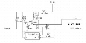
Also, as I’ve have been going through the schema for pefu’s shunt I completely missed it doesnt have a current limiter or resistor in series so it needs something between to limit a 5V supply. Facepalm. i have two sets for simpler 5v to 3.3v which will work.
I’ve decided to first attempt a doubled sided etc using the old method of laser print and transfer toner to make a power supply board.
First attempt at the ULN PCB layout.. It's funny how when you think about SMT vs THT, there's differences in the technics you use. I found myself rather annoyed at the size of the THT (the 3080 is the THT HS variant for current).
I have some parts, I have a double sided non-photo etch style PCB. I'm trying to work out if it's simply best if the ground is in the centre as a star ground. That way each regulator return current from a DC perspective will be straight to it. The high frequency will follow the paths back so I've kept the paths separate as much as possible to prevent cross talk.

I still need to have a think if this is a good layout, I'll then worry about the impedance of trace thicknesses.
I have some parts, I have a double sided non-photo etch style PCB. I'm trying to work out if it's simply best if the ground is in the centre as a star ground. That way each regulator return current from a DC perspective will be straight to it. The high frequency will follow the paths back so I've kept the paths separate as much as possible to prevent cross talk.
I still need to have a think if this is a good layout, I'll then worry about the impedance of trace thicknesses.
- Home
- Design & Build
- Equipment & Tools
- Nick's audio test system (AK5572 ADC 129KHz 32bit stereo balanced input)