So I'm happier with the above - I've tried to give the power wide low impedance tracks area to run through, the majority of the back is a ground referenced plane. The only specials are the SET pins of the 3080 that need have a guard ring, and, in this case I use both a guard pour around but also a out referenced pour to provide a reference plane instead of the ground.
Looking at at the board above from an RF noise perspective, I think the majority of the low impedance return current will through the ground plane under the wide tracks. The DC and LF return will be point to point. The optimisation is more around RF than DC given the pull through the board will be a direct result from the clock pulses. However given the previous points about the average of the clock is DC (ie the clock is AC and so cancels out on average), I'm not sure if I should be optimising for DC return current.
Now I'm looking back at my clock design and thinking (ignoring the lack of a current limiter) that I can really change the configuration for the power without it going all over the board.

Maybe tomorrow I'll lay out a new clock board with some new thinking. The parts are due to arrive tomorrow too 🙂
Well it looks like moving from the older kicad to a new v6 has managed to mess up the links and libraries (probably user error 😀).
So I’m going to start from scratch. Clean project, clean import of symbol libraries and then schematics and PCB from scratch to solve the referencing issues etc.
Now i can see why marcel doesnt want to move to v6 🙂
So I’m going to start from scratch. Clean project, clean import of symbol libraries and then schematics and PCB from scratch to solve the referencing issues etc.
Now i can see why marcel doesnt want to move to v6 🙂
So I now have all the parts for building the power board, the clock board and digital isolators. I spent the evening collating and cross referencing the parts from the two orders so I'm not using the wrong part in a project. I suppose I should have used the customer reference number in the mouser order list to separate between projects! (I wonder if they place them in different bags in the box). Also I took a liberty of purchasing a pair of shorting caps and a pair of BNC-phono adaptors which means it's working nicely for single ended as well as differential.
I'm going to restart the designs for both the power board and clock. I think it was John Cleese (Monty Python) that said you do a draft, sleep on it, throw that away, do a second draft, sleep on it again, then throw that away and the third draft you keep.
Another part I'm starting to fixate on is the front end protection. Currently I'm not DC coupled, instead each input goes through a 100V Wima 10uF MKP4. This provides 100V protection, but it does not provide AC pulse protection where the initial connection or startup of the amp goes above ~2V (4V differential). The ADC board has some protection but I think I need to calculate the amount of current that the 10uF could cause when a 100Vdc connection is plugged in or starts causing a large transient. For line level this is not an issue, but in the case of using a voltage divider to support 400V (scaled to 2 or 4V input) for tube amps, hybrids or solid state in 'oops' scenarios that may be a good idea (at least the ability to have added protection that can be switched out).
However for now - back to the power board first..
As I'm redoing the PCBs, it's occurring to me I'm making some rookie mistakes around grounding - specifically the analogue (±15V) vs digital (5V,3V) and also some other areas. I've been reading some these: https://www.powerelectronicsnews.co...t-2-power-supply-design-tutorial-section-3-2/
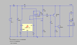
Currently I'm trying to minimise the loops - DC as well as RF. Power comes in on C24. Not finished yet - but I'm trying to place the shunt loops as small as possible (using THT) and provide a fast path of RF return. I'll also add some additional SMT pads for termination etc.

Currently I'm trying to minimise the loops - DC as well as RF. Power comes in on C24. Not finished yet - but I'm trying to place the shunt loops as small as possible (using THT) and provide a fast path of RF return. I'll also add some additional SMT pads for termination etc.

Spotted some errors in my pin connections (due to using footprints and different symbols between Kicad and ltspice). Fixed those and ran a ltspice simulation of the shunt to see if my thinking about where the main currents will be and the where the DC and RF will route.
With a 24MHz switch on the load and a 120mVpp ripple on the power source, there's absolutely no switching noise reaching the power source in the simulation. However ripple, it's not resolving the 120mV, so a LDO ahead of it will be required to remove that. This is what the power supply sees with only a few 50Hz cycles:

However I am happier with this being on the ADC digital 5V now as originally intended.
With a 24MHz switch on the load and a 120mVpp ripple on the power source, there's absolutely no switching noise reaching the power source in the simulation. However ripple, it's not resolving the 120mV, so a LDO ahead of it will be required to remove that. This is what the power supply sees with only a few 50Hz cycles:
However I am happier with this being on the ADC digital 5V now as originally intended.
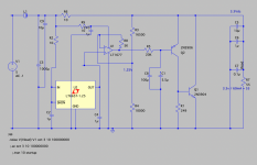
Hacked up a 3.3V shunt for the isolator on a proto board. The other side of the iso will be powered by the stm32.

So I'm getting 4V IRL out rather than 3.3 but that not a problem. I'm also reverse engineering this so I can modify to suit the purpose - I see the TL431 is used as a comparator, then we have a the NPN controlling the PNP for current control. I have an LTspice sim providing 60mA and 3.3V at the load with adjusted resistances.
I'll have a play around later tonight/tomorrow.
I'll have a play around later tonight/tomorrow.
Sorry - yes the one you shared, I've also reverse engineered so I with resistor between the output and the TL431 increased it should boost the output to cope with the slight drops for the ferrites.
Btw - thank you, that wasn't meant to be ungrateful.
Btw - thank you, that wasn't meant to be ungrateful.
I was confused since its not a shunt regulator. I have a sim of a shunt version I'll post later.
It’a simple enough to create a current shunt following this and use the LT431 to control an NPN, although there’s a tnt audio thread that compares different shunts and even battery types for noise.
First impedance (in this case compared to a LM317)
https://www.tnt-audio.com/clinica/regulators2_impedance2_e.html
Next is noise - there’a a number of pages but is also addresses the TL431 but shows a zener + 550 returning a better noise figure:
https://www.tnt-audio.com/clinica/regulators_noise3_e.html
The TL431 has little impact on the noise in the circuit above .01 Hz. The trick is to operate the NPN at its optimum for noise and the PNP handles the necessary current gain. I had to build a special test ficture with a geoformer to measure the noise. It was in the range of a 5 ohm resistor I seem to remember. Really low. The RC at the base of the NPN sets the reference noise. You do have a long turn on time. For reference attached is a shunt variation. The problem with it would be the slow turn on will mean overvoltage at turnon.
Attachments
I’m using the digital isolators as a testbed - they don’t care if it’s 5V.
Good point about the turn on overvoltage - this first one is feed a digital isolator which is happy with 3.3 and up to 5.5V but it will not operate correctly with the logic input being 3.3V (input only so no over volt output). The other side is powered by the stm 3.3V so there’s no issue. I dont thing it matters if it’s shunt or series for that.
The second digital isolator does have output to the adc, but that could be handled by a relay delay (waiting for the voltage to drop, detecting below 3.6V and then enabling) as the data transfer rate will be alot slower.
The clock on the other hand will need a overvolt protection as it’s 3.3v only


May separate completly the opamp & reference power as a separated 20V path.Also updating R5 to 10K again reduces the noise from the PNP.
Finally, add some cap switching as a load on the output, as equal on SDM ADC/DAC references (AKM) and show the switching impulse result(s) 😀
My 2 cents
Hp
- Home
- Design & Build
- Equipment & Tools
- Nick's audio test system (AK5572 ADC 129KHz 32bit stereo balanced input)