Start with a current source- not a voltage source. The 10 Ohm resistor is the source impedance and passes a lot of current. Not the best use of a shunt rregulator. The principle (ref schematic attached) is to sense the output voltage compared to a reference and then pull the base of the PNP negative to pull the sensed voltage (shunt) down. However in this application you have two nested regulators. The voltage reference which slowly monitors the output and will correct for changes in Vbe from load and temperature but the low noise comes from the PNP-NPN pair. The difference between the base and emitter of the PNP is amplified to the base of the NPN which pulls additional current to regulate the voltage. The noise is really that of the input transistor not of the opamp. Shunt regulators are best for applications with very predictible and limited current requirements.
Attached is a 3.5V shunt version. The power disspation of the NPN would need to be managed.
Attached is a 3.5V shunt version. The power disspation of the NPN would need to be managed.
Attachments
Yup that’s my next step 24Mhz switching. I have some ferrites targetting that to see if it’s stable with those in the output.May separate completly the opamp & reference power as a separated 20V path.
Finally, add some cap switching as a load on the output, as equal on SDM ADC/DAC references (AKM) and show the switching impulse result(s) 😀
My 2 cents
Hp
The npn be parallelled.Start with a current source- not a voltage source. The 10 Ohm resistor is the source impedance and passes a lot of current. Not the best use of a shunt rregulator. The principle (ref schematic attached) is to sense the output voltage compared to a reference and then pull the base of the PNP negative to pull the sensed voltage (shunt) down. However in this application you have two nested regulators. The voltage reference which slowly monitors the output and will correct for changes in Vbe from load and temperature but the low noise comes from the PNP-NPN pair. The difference between the base and emitter of the PNP is amplified to the base of the NPN which pulls additional current to regulate the voltage. The noise is really that of the input transistor not of the opamp. Shunt regulators are best for applications with very predictible and limited current requirements.
Attached is a 3.5V shunt version. The power disspation of the NPN would need to be managed.
Start with a current source- not a voltage source. The 10 Ohm resistor is the source impedance and passes a lot of current. Not the best use of a shunt rregulator. The principle (ref schematic attached) is to sense the output voltage compared to a reference and then pull the base of the PNP negative to pull the sensed voltage (shunt) down. However in this application you have two nested regulators. The voltage reference which slowly monitors the output and will correct for changes in Vbe from load and temperature but the low noise comes from the PNP-NPN pair. The difference between the base and emitter of the PNP is amplified to the base of the NPN which pulls additional current to regulate the voltage. The noise is really that of the input transistor not of the opamp. Shunt regulators are best for applications with very predictible and limited current requirements.
Attached is a 3.5V shunt version. The power disspation of the NPN would need to be managed.
I've had my head stuck in alot of materials (some LT, some TI and some university papers). I see how this should work now building from a low noise current source. Also to reduce noise further - targeting low noise resistors for R1 is required. I also see that with the high speed switching I may need to have a look at the inductance in the resistor choices too. However for this purpose I don't think Vishay precision resistors with low noise (maybe MELF would suffice), I suspect it's good enough to have an accurate & precise logic chronographic cross over point that has equal timing for rise and fall without having varying slew rates.
Start with a current source- not a voltage source. The 10 Ohm resistor is the source impedance and passes a lot of current. Not the best use of a shunt rregulator. The principle (ref schematic attached) is to sense the output voltage compared to a reference and then pull the base of the PNP negative to pull the sensed voltage (shunt) down. However in this application you have two nested regulators. The voltage reference which slowly monitors the output and will correct for changes in Vbe from load and temperature but the low noise comes from the PNP-NPN pair. The difference between the base and emitter of the PNP is amplified to the base of the NPN which pulls additional current to regulate the voltage. The noise is really that of the input transistor not of the opamp. Shunt regulators are best for applications with very predictible and limited current requirements.
Attached is a 3.5V shunt version. The power disspation of the NPN would need to be managed.
Well, I started to simulate using a dynamic switching load as ~1mA (resistor) with a serial 100pF load to GND and shorted only as 0.02us on....
the alternate LDO I used was the known LT3042.
The question rises about a common/regular used switching load and timings... so I am not completely off the rules 😀
Hp
The circuit I shared is well suited to crystal oscillators since they are a "perfect" static load. The goal was the lowest noise on the supply of the crystal, which can be seen in the plase noise plots. They are not suitable for dynamic loads like audio. Maybe for the Vref of a DAC when coupled to a really large cap with low ESR.
OK, I name also OXCO as a possible target as 500mA/cold down may to 100mA/hot.
Once I simulated with a current source as 0.3A (oposite to 20V 1K), using on LTSpice, the output started to oscillate. Current source as on 0.05A was quiet.
Nick will soon or later on the REF task, as ADC with REF switching cap(s).
Once I simulated with a current source as 0.3A (oposite to 20V 1K), using on LTSpice, the output started to oscillate. Current source as on 0.05A was quiet.
Nick will soon or later on the REF task, as ADC with REF switching cap(s).
So i managed to try using transparencies and transfer laser toner over onto copper FR4 using the mrs’ cricut press. That worked but it needs a number of overlaid toner layers and the laser printer has a grid appearance once transferred (i think that’s the laserprinter toner deposition). I messed that by not having the back misaligned. So for the voltage regulators (+/-15V and 5V) I just protoboarded them.
With 22uF on the set pin they adjust slowly to the trim pot and start up, but settle and seem stable on the bryman on 500K count mode.
I’ll try on the ADC this weekend to see if the 100Hz disappears.
I may simply say blow it and jlcpcb the clock boards and a batch of regulators. I will try the photo etch with the lessons learnt from the standard process but i’m thinking my patience may run to protoboards then ordering pcbs! (Especially with summer DIY season arriving)
SMPS noise input..

Noise (without ferrites) at the shunt output for the isolation - note the cursors remain the same scale. Also there's no shielding on the desk:

So the SMPS has a 120mVpp rating, that's reduced nicely, next will be adding a little more LF and HF filtering.
I'll order the other shunt's components and then sort out the design on the PCB for the clock.
Noise (without ferrites) at the shunt output for the isolation - note the cursors remain the same scale. Also there's no shielding on the desk:
So the SMPS has a 120mVpp rating, that's reduced nicely, next will be adding a little more LF and HF filtering.
I'll order the other shunt's components and then sort out the design on the PCB for the clock.
Last edited:
As expected adding some ferrite goodness kills a large amount of the noise - there's some spikes but the broader noise seems to have been attenuated nicely.

It's odd that the spikes are not at some high frequency but at 50Hz. So I'm wondering if that's coming in from the SMPS rectification! It may be that SMPS is underloaded, even with the shunt and the isolation chip connected.
It's odd that the spikes are not at some high frequency but at 50Hz. So I'm wondering if that's coming in from the SMPS rectification! It may be that SMPS is underloaded, even with the shunt and the isolation chip connected.
Are you measuiring differentially? There are noise sources that can get into measurements and really confuse. I start this with differential measurement and short the probe tips at the point of measurement to make sure I'm looking a real stuff. The 50 Hz spikes could be magnetic and not conducted.
There's lots of noise - this is the two probes not connected but connected together & with grounding connected measuring difference between the two probe measurements:
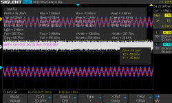
SMPS+3080 before the shunt (this is the original 5V to 4V shunt with 3.3V passed through) - I'm measuring ground and Vdd.
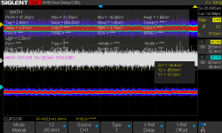
Then post shunt and ferrites, same ground and Vdd:
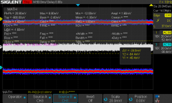
I put the Brymen after the above in the circuit and it's reading just over 1.5mA with 0.0011 mA delta between readings. I think I'm getting to the limit of my equipment in the noisy configuration I've got on the desk. Perhaps it's time for me to make some changes to the desk for better noise.
I think the next step is to get the clock+shunt boards designed and etched. Failing that get the Gerber's over to jclpcb. I've got some SMT 3080 and 3042s that I want to have some regulator PCBs available for future projects so I may make use of their prototype services to save time.

SMPS+3080 before the shunt (this is the original 5V to 4V shunt with 3.3V passed through) - I'm measuring ground and Vdd.

Then post shunt and ferrites, same ground and Vdd:

I put the Brymen after the above in the circuit and it's reading just over 1.5mA with 0.0011 mA delta between readings. I think I'm getting to the limit of my equipment in the noisy configuration I've got on the desk. Perhaps it's time for me to make some changes to the desk for better noise.
I think the next step is to get the clock+shunt boards designed and etched. Failing that get the Gerber's over to jclpcb. I've got some SMT 3080 and 3042s that I want to have some regulator PCBs available for future projects so I may make use of their prototype services to save time.
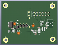
Update with the new shunt - note that I've made the reference divider a quad ladder to reduce current but, I don't think it will be required. I've also used three NPNs in parallel to shunt, the DC path is straight from the power resistor back to the ground (same with the PNP and the reference) on the opposite side from high frequency. Trying to get the smallest loop for the largest current then leaving the HF return path without having any shut DC crossing it.
It's also occurred to me that my power supplies (two SMPS bench supplies) are plugged into a separate wall socket - so earth ground from those will have a very large loop from the scope that is plugged into a different wall socket (they're on the same upstairs loop). It would be better if they're plugged next to each other, whilst the Mac, work laptop etc are plugged on the other wall socket connection. I will try that later.
Last edited:
Nick, do you have the actual LTSpice asc file for sharing, as I like to do some pulse related simulations. As I did with Salas.
This is the basic form - note I may alter the caps etc:

There's at least two 10uF caps that can go.
L2 is a 200mDCR but 600R 100MHz inductor, and the configurations for the coupled ferrites are 20mDCR but 175R 100MHz (ltspice) optimised for 25MHz.
Moving the plugs around has halved the noise on the shorted test!
There's at least two 10uF caps that can go.
L2 is a 200mDCR but 600R 100MHz inductor, and the configurations for the coupled ferrites are 20mDCR but 175R 100MHz (ltspice) optimised for 25MHz.
Moving the plugs around has halved the noise on the shorted test!
Last edited:
Hmm, hardly to to convert you given picture to modify the current asc LTSpice file.
As it currently shows as using previous as may similar posted, not that good as compared to real as Salas one.
I cannot tell how, the given Shunt regulators as the old Broberly or Tenlabs (the smart sized) performs.
Important also the voltage stabilization as a otherwise a pitta on ADC/DAC reference inputs.
Just my 2 cents
For now I don’t have to worry about rhe ADC vref or the RTZ DAC voltage reference, just the clock which should be fine except for noise and current loop induced ground bounce between the boards which i hope will not be an issue.
I think you have q4 upside down and the wrong polarity. The emitter should be tied to the voltage and the collector drive the NPN's. When the regulated voltage changes it in(de)creases the voltage between the base and emitter and the collector current from the change turns on (off) the NPN's.
- Home
- Design & Build
- Equipment & Tools
- Nick's audio test system (AK5572 ADC 129KHz 32bit stereo balanced input)
