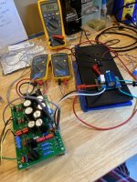
Thanks for posting this simple, neat little preamp circuit ra7. I decided to have a go at your resistor loaded version and cobbled together one channel built with 19N20/12P20 mosfets. Initial power up was with 90v and 37mA (RL=1K, 5W). This sounded pretty darn good on my bench speaker. With your recommendation, I bumped V+ up to 110V and current to 55mA. This increase created a burning hot 5watter!! I spread the dissipation over 4 resistors in parallel/series. The sound got even better with these setpoints. I built a second channel and will soon have stereo listening. Lots of good input tweaks from other members also, looking forward to more positive improvements to SCG Preamp 🙂
Attachments
One novice question , is this arraingement of using 2nd mosfet in common gate configuration , same as cascode arraingement ?? Are both same ..
Introducing the Schade Common Gate (SCG) Preamp. Signal comes in at the bottom source follower (unity voltage gain) and is then amplified by the Schade-enabled top MOSFET operated in a common gate configuration. This gets around the problem of low impedance on the gate of the Schade device. Inspiration came from George (tubelab) and Smoking-Amp, who were exploring the source-follower to common gate configuration for tube pentodes. I made a comment here that you could do this with MOSFETs too.
CCS Version
The CCS-loaded version’s performance is out of this world for a single gain transistor. Subjectively, it sounds very sweet and clean, but somewhat recessed. On loud symphonic pieces and rock music, it sounds better, but on quieter stuff, it doesn’t quite have the presence and 3D-ness of the resistor-loaded version. This is kind of an amazing subjective result and shows that we (or at least me) probably want quite a bit of that negative phase H2.
I have built something similar to both of these. I also have a three device version with a tube pentode in place of the middle mosfet. All use a single IXCP10M45 or 10M90 for the CCS. They were built with a somewhat different purpose in mind. I need a low distortion driver stage capable of hundreds of volts of output.
Almost 15 years ago I applied some of the RF power amp work I was doing in my day job to a single ended vacuum tube audio amp. Most SE amps are limited in power output by the dissipation in the output device. If we could remove that limitation more power could be obtained from a given device. At that time class G and class H push pull audio power amps existed. My work applied this technology to single ended RF power amps used in cell towers and phones to improve the efficiency. For this to work the output stage must have a high PSRR. In the audio world this means a source or cathode follower topology, which has no voltage gain, hence the requirement for a driver stage capable of lots of voltage swing in a tube amp. This should be far easier in a solid state design.
The work I did long ago was for a design contest sponsored by Microchip in Circuit Cellar magazine. It resulted in a SE class A (really class H) vacuum tube amplifier that easily doubled the power output usually obtained from the same tube used in a conventional SE amp design. The magazine article has fallen off of Circuit Cellar's website, so I am including it here. I am the author.
In that design the output stage is a cathode follower. I applied some techniques using a mosfet source follower on top of the cathode follower to improve its PSRR. These concepts come from work done (and patented) by Ross MacDonald in the 1950's. This concept was discussed almost 15 years ago. It could all be built with semiconductors and scaled up in power, but my version is a hybrid. It is here:
https://www.diyaudio.com/community/threads/augmented-cathode-follower.114021/
and , with that arrangement, you can alter THD with ease
as some Greeedy Boyz are often asking - can I put multiswitch there?
and as I'm often replying - get it done right once, you'll stop fiddling .......

I built a guitar amp with a CCS loaded pentode in the input stage for super high gain. It had several pots in it for maximum tweakability. I would sit down with my guitar and turn pots forever before finally finding the sound that I wanted. I went through this loop several timed over a week or two before I realized that it was impossible to reach convergence. I then set out to eliminate one pot at a time. It took nearly a month, but the amp now exists in completed form with one pot on the front panel. I have often wanted to go back inside for more fiddling, but so far, I have resisted the temptation.
One could also put a pot in series with that bypass cap across the 10K trimpot.......considering that Iq/biasing is set either with resistor or CCS, feel free to play with Schade resistor values, thus changing transfer function by your liking
also - voltage potential for upper mosfet - I prefer it firm as possible, at least in AC domain ....... meaning - I believe it is good having decent elco across 10K trimpot
in my shenanigans (difference - not line stages) , I did found 750R and 18K as nice Schade combo ......
Attachments
Thanks for posting this simple, neat little preamp circuit ra7. I decided to have a go at your resistor loaded version and cobbled together one channel built with 19N20/12P20 mosfets. Initial power up was with 90v and 37mA (RL=1K, 5W). This sounded pretty darn good on my bench speaker. With your recommendation, I bumped V+ up to 110V and current to 55mA. This increase created a burning hot 5watter!! I spread the dissipation over 4 resistors in parallel/series. The sound got even better with these setpoints. I built a second channel and will soon have stereo listening. Lots of good input tweaks from other members also, looking forward to more positive improvements to SCG Preamp 🙂
Congrats Vunce! Your build is much spiffier than mine. Let us know how the listening goes!
No, it is not a cascode because the bottom MOSFET is operated in a source follower configuration.One novice question , is this arraingement of using 2nd mosfet in common gate configuration , same as cascode arraingement ?? Are both same ..
Our George!as always, our George at his best
🙂

Thanks for the article! I believe Bill Waslo did something similar in Linear Audio, though I haven't read it:I have built something similar to both of these. I also have a three device version with a tube pentode in place of the middle mosfet. All use a single IXCP10M45 or 10M90 for the CCS. They were built with a somewhat different purpose in mind. I need a low distortion driver stage capable of hundreds of volts of output.
Almost 15 years ago I applied some of the RF power amp work I was doing in my day job to a single ended vacuum tube audio amp. Most SE amps are limited in power output by the dissipation in the output device. If we could remove that limitation more power could be obtained from a given device. At that time class G and class H push pull audio power amps existed. My work applied this technology to single ended RF power amps used in cell towers and phones to improve the efficiency. For this to work the output stage must have a high PSRR. In the audio world this means a source or cathode follower topology, which has no voltage gain, hence the requirement for a driver stage capable of lots of voltage swing in a tube amp. This should be far easier in a solid state design.
The work I did long ago was for a design contest sponsored by Microchip in Circuit Cellar magazine. It resulted in a SE class A (really class H) vacuum tube amplifier that easily doubled the power output usually obtained from the same tube used in a conventional SE amp design. The magazine article has fallen off of Circuit Cellar's website, so I am including it here. I am the author.
In that design the output stage is a cathode follower. I applied some techniques using a mosfet source follower on top of the cathode follower to improve its PSRR. These concepts come from work done (and patented) by Ross MacDonald in the 1950's. This concept was discussed almost 15 years ago. It could all be built with semiconductors and scaled up in power, but my version is a hybrid. It is here:
https://www.diyaudio.com/community/threads/augmented-cathode-follower.114021/
I built a guitar amp with a CCS loaded pentode in the input stage for super high gain. It had several pots in it for maximum tweakability. I would sit down with my guitar and turn pots forever before finally finding the sound that I wanted. I went through this loop several timed over a week or two before I realized that it was impossible to reach convergence. I then set out to eliminate one pot at a time. It took nearly a month, but the amp now exists in completed form with one pot on the front panel. I have often wanted to go back inside for more fiddling, but so far, I have resisted the temptation.
One could also put a pot in series with that bypass cap across the 10K trimpot.......
https://linearaudio.net/volumes/2269
Regarding that last comment about the trimpot: are you proposing using a trimpot instead of the 1k feedback resistor? That would be neat. We could listen to different levels of feedback. Right now, it is at 10% (R2 = 10k, R1 = 1k). It results in pretty vertical, evenly spaced curves.
I did some horsing around with different levels of feedback, trying out 680 and 10k, and 680 and 20k, and still got pretty vertical and evenly spaced curves. But a pot would make this process easier.
In my experiments with a similar design having a vacuum tube pentode in the middle position I also found that 10 to 12% feedback seemed to work best.Regarding that last comment about the trimpot: are you proposing using a trimpot instead of the 1k feedback resistor? That would be neat. We could listen to different levels of feedback. Right now, it is at 10% (R2 = 10k, R1 = 1k). It results in pretty vertical, evenly spaced curves.
I did some horsing around with different levels of feedback, trying out 680 and 10k, and 680 and 20k, and still got pretty vertical and evenly spaced curves. But a pot would make this process easier.
The tube pentode functions much like a depletion mode mosfet with a pinchoff voltage in the 20 to 50 volt range. Here I did not need the 100K to B+, so my feedback divider is just two resistors. Changing the feedback ratio affects both AC feedback, and DC bias. In order to make testing a bit easier I set the resistor divider to get me somewhere over 15% feedback, then added a series pot and cap from grid to ground to shunt a variable amount of AC feedback to ground without affecting the DC of the chain.
In my experiments with a similar design having a vacuum tube pentode in the middle position I also found that 10 to 12% feedback seemed to work best.
The tube pentode functions much like a depletion mode mosfet with a pinchoff voltage in the 20 to 50 volt range. Here I did not need the 100K to B+, so my feedback divider is just two resistors. Changing the feedback ratio affects both AC feedback, and DC bias. In order to make testing a bit easier I set the resistor divider to get me somewhere over 15% feedback, then added a series pot and cap from grid to ground to shunt a variable amount of AC feedback to ground without affecting the DC of the chain.
So, like this:
Could use a depletion mode MOSFET like DN2535 or similar. Maybe save one from the CCS and use it here😉
Thanks! Great ideas.
I have also been experimenting with other FETs in both positions, especially ones with low gate capacitance, and have some promising results.
Yes, that is exactly what I built with a tube in the middle position. A small capacitor across R2 may be needed with a mosfet to compensate for gate capacitance.
I built my triple fet version with an IXYS IXTP3N100D2 in the middle position. It is a depletion mode part, but again I chose it for a different reason, an enhancement mode fet will work too as long as the DC bias is worked out. I was also running 650 volts of B+.
For many years it was assumed that mosfets were immune to the secondary breakdown failure mechanism seen in BJT's. We now know that is not entirely true. A secondary breakdown mechanism does exist in mosfets. It is somewhat different than the failure mode seen in BJT's and has become worse as mosfets are optimized for faster operation in switching applications. The RF design team I worked in at Motorola spent nearly two years chasing this down with lots of expensive Flir thermal video equipment in some specialized GaN RF power amp parts. GaN is worse than silicon in this respect due to its higher thermal resistance. This is why many GaN parts are built on a SiC substrate. The failure mechanism is related to thermal hot spots on the die and the localized increase in RDSon in a hot spot.
It is currently believed that depletion mode parts have a far greater resistance to this kind of failure than enhancement mode parts when operated as a linear amplifier. This failure mechanism gets worse as the drain - source voltage is increased. Many vendors (Onsemi) still do NOT recognize this failure mechanism in their data sheets. If the DC curve in the SOA plot is exactly the same as the part's rated dissipation, or there is no DC curve, it will fail if used continuously in linear operation, often far below its rated dissipation. It may take a minute, or it may take a year, and some parts will run forever, but some will eventually die. I have been testing a big tube amp that makes 250 watts per pair of tubes. The P channel mosfet under the cathode in that application has failed in spectacular fashion a few times. Here the idle voltage across the fet is 70 to 80 volts and peak currents are over 1 amp. These conditions do not occur simultaneously, but many parts will fail here even when operated well inside their ratings. The best garden variety mosfet that I have tested so far is the Onsemi FQPF9P25.
This failure has been seen by myself and others in the tube amp community when using mosfets as linear voltage regulators at high, but well within spec, voltages. IXYS, Exicon and a few others make mosfets specifically designed for operation as linear amplifiers or regulator pass devices. I have several to test but haven't gotten to it yet. In a low current preamp application that runs on 100 volts or so, there is likely no issue, but driving a reactive speaker load directly at a reasonable power level may be a different story.
In this circuit the current is constrained by the CCS. The characteristics of the middle device and its gate, grid, or base voltage will determine the idle voltage on the bottom device. The bottom device needs enough voltage across it to remain linear across the entire expected drive levels. 4 to 5 volts may be OK for low level signals, but simulations revealed distortion at the source of the fet without a bit more voltage with line level inputs. I wound up with about 10 volts on the gate which required a capacitor on the input.
How do I calculate the value of that R2 bypass cap?Yes, that is exactly what I built with a tube in the middle position. A small capacitor across R2 may be needed with a mosfet to compensate for gate capacitance.
Wow!I built my triple fet version with an IXYS IXTP3N100D2 in the middle position. It is a depletion mode part, but again I chose it for a different reason, an enhancement mode fet will work too as long as the DC bias is worked out. I was also running 650 volts of B+.
For many years it was assumed that mosfets were immune to the secondary breakdown failure mechanism seen in BJT's. We now know that is not entirely true. A secondary breakdown mechanism does exist in mosfets. It is somewhat different than the failure mode seen in BJT's and has become worse as mosfets are optimized for faster operation in switching applications. The RF design team I worked in at Motorola spent nearly two years chasing this down with lots of expensive Flir thermal video equipment in some specialized GaN RF power amp parts. GaN is worse than silicon in this respect due to its higher thermal resistance. This is why many GaN parts are built on a SiC substrate. The failure mechanism is related to thermal hot spots on the die and the localized increase in RDSon in a hot spot.
It is currently believed that depletion mode parts have a far greater resistance to this kind of failure than enhancement mode parts when operated as a linear amplifier. This failure mechanism gets worse as the drain - source voltage is increased. Many vendors (Onsemi) still do NOT recognize this failure mechanism in their data sheets. If the DC curve in the SOA plot is exactly the same as the part's rated dissipation, or there is no DC curve, it will fail if used continuously in linear operation, often far below its rated dissipation. It may take a minute, or it may take a year, and some parts will run forever, but some will eventually die. I have been testing a big tube amp that makes 250 watts per pair of tubes. The P channel mosfet under the cathode in that application has failed in spectacular fashion a few times. Here the idle voltage across the fet is 70 to 80 volts and peak currents are over 1 amp. These conditions do not occur simultaneously, but many parts will fail here even when operated well inside their ratings. The best garden variety mosfet that I have tested so far is the Onsemi FQPF9P25.
I'm currently trying out the STQ1N60 in the middle position.
https://www.mouser.com/ProductDetail/511-STQ1NK60ZR-AP
I bought it based on its low gate capacitance chart in the datasheet.
They are claiming quite a lot of power for the TO-92 package. Running it at 10 mA and 60 V, which is 0.6 W and even that may be pushing it but it hasn't blown-up yet. Also running a VP0106 in the P-channel position.
Yes, I can imagine running into a reactive load would be more of an issue. Have you seen Nelson's idea for a Schade power amp?This failure has been seen by myself and others in the tube amp community when using mosfets as linear voltage regulators at high, but well within spec, voltages. IXYS, Exicon and a few others make mosfets specifically designed for operation as linear amplifiers or regulator pass devices. I have several to test but haven't gotten to it yet. In a low current preamp application that runs on 100 volts or so, there is likely no issue, but driving a reactive speaker load directly at a reasonable power level may be a different story.
https://www.diyaudio.com/community/threads/50w-single-ended-baf2015-schade-enabled.290776/
In this circuit the current is constrained by the CCS. The characteristics of the middle device and its gate, grid, or base voltage will determine the idle voltage on the bottom device. The bottom device needs enough voltage across it to remain linear across the entire expected drive levels. 4 to 5 volts may be OK for low level signals, but simulations revealed distortion at the source of the fet without a bit more voltage with line level inputs. I wound up with about 10 volts on the gate which required a capacitor on the input.
That makes sense. With the STF part above and the gate of the bottom part at 0 V, I am getting about 3V on the source pin of the bottom part. This remains fairly constant as I sweep the drain voltage on the middle part. Still learning how to bias up these different devices.
I am getting clean 25 V peak-to-peak swing in the above setup. That's as high as I can test right now. See chart below. The one that is clipping is a 10Y tube preamp and the reason for clipping is that the gyrator load doesn't have even voltage difference on it (it has about 20 V)--though I haven't tested that theory yet.
The cap value would depend on the gate capacitances of the mosfet which will vary with applied voltage. The reason for the cap across R2 is to compensate for the low pass filter created with R2 and the gate capacitance. I would tend to get the amp working and then look at the high frequency response, or just apply a 5 to 10 KHz square wave to the input and tweak for the best square wave at the output.How do I calculate the value of that R2 bypass cap?
I simulated the UNSET design in LT Spice and got it to work there before building one. I used some random p channel mosfet that was already in the library for my sims. That part turned out to be SMD, so I bought a bunch of similar mosfets in TO-92 to try. The VP0106 was the first one I tried, and it worked, so I never got to the rest. Someday I will find out if the others make any difference.I'm currently trying out the STQ1N60 in the middle position. I bought it based on its low gate capacitance chart in the datasheet.
They are claiming quite a lot of power for the TO-92 package. Running it at 10 mA and 60 V, which is 0.6 W and even that may be pushing it but it hasn't blown-up yet. Also running a VP0106 in the P-channel position.
I did not know about that part. I'll get some next time I order parts since I have been running LND150's over their voltage spec in applications where an enhancement fet will also work (phase splitters in tube amps).
The data sheet isn't clear if 3 watts were on an infinite heat sink what, but with a Rthj-amb of 120 C/W one watt would put the die in the 150C range. The Rthj-lead of 40 C/W might allow two watts or so if the leads were short and went into some serious copper on a PC board. 0.6 W should be OK.
I did not know about that amp. The first thing that pops into my mind is the application of feedback in series with the input. I guess it's OK, but the source would need to be a pretty low impedance.Yes, I can imagine running into a reactive load would be more of an issue. Have you seen Nelson's idea for a Schade power amp?
I can envision a complete UNSET amp design with no tubes. There are some serious SiC fets rated for 700 volts available today for about the same price as a big tube ($20). I doubt that I will ever build it due to the flak that it would draw. Nearly 20 years ago I used a mosfet source follower to drive the grid of a 300B triode in an amp I called the TSE. When I posted it here and elsewhere on the web the response was overwhelmingly negative. Some even suggested changing my name to Transistorlab. Little by little people built them and liked them. Someone took one to BAF and the Transistorlab flak went away overnight. Today I still sell quite a few TSE-II boards. Sticking "sand" into a tube amp will always draw flak from the purists, much like stuffing an all electric drivetrain into a 1957 Chevy. Progress is slow to be adopted by some. An all silicon anti-tube amp with an OPT is much like the 57 Chevy that was debuted at this year's SEMA show.
Given a number of recent amps that include choke loads of some sore (MoFo, LuFo, etc), plus the transformer gain stages in the M2x and Diy VFET amp, one might think there would be more acceptance of iron in the signal path. It is fairly well known that a significant portion of the sound of tube-based amps comes from the output transformers. Not to mention the types of rectifiers. So it seems pretty reasonable that a high voltage FET gain stage driving a nice output transformer could be a beautiful thing.
Loudspeakers are high current low voltage devices. So, it seems logical to drive them directly with a source follower, which can be very linear. I personally went on this preamp mission because I had just built the F4, a source follower, which really lets the preamp make the sound.
Have you seen the Arch Nemesis?
https://www.firstwatt.com/pdf/art_arch_nemesis.pdf
Have you seen the Arch Nemesis?
https://www.firstwatt.com/pdf/art_arch_nemesis.pdf
As usual, Nelson delivers wonderful insight with his article. Thanks for that link.
I'm in the (long) process of building a common drain SIT follower with a choke load at the source. Who knows, maybe there is a high voltage sweet spot to be explored by substituting the choke load with a single-ended style output transformer?
I'm in the (long) process of building a common drain SIT follower with a choke load at the source. Who knows, maybe there is a high voltage sweet spot to be explored by substituting the choke load with a single-ended style output transformer?
I can envision a complete UNSET amp design with no tubes. There are some serious SiC fets rated for 700 volts available today for about the same price as a big tube ($20). I doubt that I will ever build it due to the flak that it would draw. Nearly 20 years ago I used a mosfet source follower to drive the grid of a 300B triode in an amp I called the TSE. When I posted it here and elsewhere on the web the response was overwhelmingly negative. Some even suggested changing my name to Transistorlab. Little by little people built them and liked them. Someone took one to BAF and the Transistorlab flak went away overnight. Today I still sell quite a few TSE-II boards. Sticking "sand" into a tube amp will always draw flak from the purists, much like stuffing an all electric drivetrain into a 1957 Chevy. Progress is slow to be adopted by some. An all silicon anti-tube amp with an OPT is much like the 57 Chevy that was debuted at this year's SEMA show.
You need to spend more time in the Pass Labs forum with da greedy boyz
will reply with more later today.
That sounds like fun. Let us know how it goes.As usual, Nelson delivers wonderful insight with his article. Thanks for that link.
I'm in the (long) process of building a common drain SIT follower with a choke load at the source. Who knows, maybe there is a high voltage sweet spot to be explored by substituting the choke load with a single-ended style output transformer?
bunch of ..... WeaklingsesssssYou need to spend more time in the Pass Labs forum with da greedy boyz
......
 But compared to what George deals with in his tubelab, 1 kV, etc., yeah, we are weaklingsesssss...
Okay, I will try that. Right now, the one with the STQ and VP0106 parts is sounding really good, matching the 10Y pre, which is no small feat. I really hope Vunce and others report on the sound, otherwise, it's just me tooting my own horn.The cap value would depend on the gate capacitances of the mosfet which will vary with applied voltage. The reason for the cap across R2 is to compensate for the low pass filter created with R2 and the gate capacitance. I would tend to get the amp working and then look at the high frequency response, or just apply a 5 to 10 KHz square wave to the input and tweak for the best square wave at the output.
With the STQ part in the middle position and about 60 V on the drain and 10 mA, I am getting about 0.05% distortion at about 2 Vrms, which is just right for me. It is heavily 2nd harmonic, with just a teeny bit of 3rd.
Yeah, I looked at your UNSET schematic and picked up some VP0106 to try. ZM also suggested TP2640 and I got those too. I also literally stared at the 26,000 or so MOSFETs on offer at MOSFETs and came up with a few more options, searching for the phrase "low gate capacitance" in the search within results.I simulated the UNSET design in LT Spice and got it to work there before building one. I used some random p channel mosfet that was already in the library for my sims. That part turned out to be SMD, so I bought a bunch of similar mosfets in TO-92 to try. The VP0106 was the first one I tried, and it worked, so I never got to the rest. Someday I will find out if the others make any difference.
There are some cool parts out there with nice pentode curves and some funky looking curves between a pentode and triode.
Good to know. I am going to put this on a solder breadboard and may try to push more mA through it.I did not know about that part. I'll get some next time I order parts since I have been running LND150's over their voltage spec in applications where an enhancement fet will also work (phase splitters in tube amps).
The data sheet isn't clear if 3 watts were on an infinite heat sink what, but with a Rthj-amb of 120 C/W one watt would put the die in the 150C range. The Rthj-lead of 40 C/W might allow two watts or so if the leads were short and went into some serious copper on a PC board. 0.6 W should be OK.
You should totally do this and I'm sure it will be well received here. I don't see why Transistorlab and Tubelab couldn't coexist.I can envision a complete UNSET amp design with no tubes. There are some serious SiC fets rated for 700 volts available today for about the same price as a big tube ($20). I doubt that I will ever build it due to the flak that it would draw. Nearly 20 years ago I used a mosfet source follower to drive the grid of a 300B triode in an amp I called the TSE. When I posted it here and elsewhere on the web the response was overwhelmingly negative. Some even suggested changing my name to Transistorlab. Little by little people built them and liked them. Someone took one to BAF and the Transistorlab flak went away overnight. Today I still sell quite a few TSE-II boards. Sticking "sand" into a tube amp will always draw flak from the purists, much like stuffing an all electric drivetrain into a 1957 Chevy. Progress is slow to be adopted by some. An all silicon anti-tube amp with an OPT is much like the 57 Chevy that was debuted at this year's SEMA show.
After I'm off this preamp kick, I am going to scale this up and build a power amp version of the preamp. No more unobtanium triodes.

Yeah, my momentum stalled a bit while building a HV shunt psu. Had to order caps with correct voltage ratings, should be listening in stereo by the end of the week. In the meantime I'm enjoying your journey 🙂
......
After I'm off this preamp kick, I am going to scale this up and build a power amp version of the preamp. No more unobtanium triodes.
one of best versions is already made .......

it's called DEFiSIT ....... then all of its derivatives
of course, not saying that field is exhausted ...... 🙂
- Home
- Amplifiers
- Pass Labs
- Schade Common Gate (SCG) Preamp