I go up a diode from the supply through D5. Without D1, the base of the drivers would go a diode above the supply during clipping. I think saturation would be possible and quasi-saturation would be inevitable, probably leading to ringing as the drivers exit quasi-saturation. I mean, that's the whole point of having the diodes, right?I dont use D1, but my "diamond" is a bit different.
That's big talk for someone who hasn't simulated my amplifier. How would you recommend to compensate a folded cascode amplifier?I haven't simulated your amplifier, but I think that you are "killing" a lot of gain by your compensation.
In an FC amplifier, Miller has to be input inclusive, and the gain of the stage is just too high for that to work right on this amplifier. Trust me, I've tried. That rules out two-pole compensation, and output inclusive compensation becomes part of the global feedback. Right now, the 0 dB loop gain crossing is just under 5 MHz.
The only other FC amplifier I've seen on diyaudio is roender's RMI-FC100. He started by using 30 pF of output compensation on the FC, and then switched over to 4 pF of Miller input compensation. The FC100 loop gain is about 15 dB lower than mine, so he got that to work OK. I could not.
In simulations, I'm not seeing any nonlinearity due to charging/discharging of the 36 pF of compensation cap. My nonlinearity is dominated by the output stage, at this point. That is why I think ojg is on the right track, suggesting a CFP for the OPS.
That will likely kill a bit of my overall loop gain, but make up for it with local feedback in the CFP. With lower loop gain, that phase lead compensation may be workable. Roender also used a CFP OPS.
Hi stinius,
I was able to try the flying baker clamps, and it did help a little. In simulation:
20 kHz, 100W THD dropped 8%, from 0.0019% to 0.00175%
20 kHz, 200W THD dropped 9.3%, from 0.0054% to 0.0049%
If I stay with the triple EF and diamond pre-driver, this is where these diodes live now. Thanks for the suggestion. As I say, I had not considered it.
Normally I would use shunt compensation on the VAS output for folded cascode but it looks like you are already doing that.
Check out figure 31 on page 9 and read the theory of operation. I haven't tried this personally yet though.
Check out figure 31 on page 9 and read the theory of operation. I haven't tried this personally yet though.
Attachments
Last edited:
Hi stinius,
I was able to try the flying baker clamps, and it did help a little. In simulation:
20 kHz, 100W THD dropped 8%, from 0.0019% to 0.00175%
20 kHz, 200W THD dropped 9.3%, from 0.0054% to 0.0049%
If I stay with the triple EF and diamond pre-driver, this is where these diodes live now. Thanks for the suggestion. As I say, I had not considered it.
Hi Russell
That's good, everything matters.
Adding 2 diodes and achieve close to 10% reduction in THD@ 20k seems ok to me.
BTW: did you use D1 or did you delete it?
In my opinion you should stick to the 3 EF diamond.
Stein
Last edited:
I kept D1. I need it to keep the drivers from saturating.
Thanks for the vote of confidence. I'm not really married to the 3EF, but the diamond has been working well. I went that way originally for maximum OPS bandwidth.
Thanks for the vote of confidence. I'm not really married to the 3EF, but the diamond has been working well. I went that way originally for maximum OPS bandwidth.
Normally I would use shunt compensation on the VAS output for folded cascode but it looks like you are already doing that.
Yep. That's what they taught me at op-amp school.
Check out figure 31 on page 9 and read the theory of operation. I haven't tried this personally yet though.
In op amp school (Texas Instruments experience on the job), we used simple shunt compensation if the output stage was a follower. However, it was usually a push-pull common-source output for rail-to-rail operation. We would string a Miller C across the output transistors back to the FC output node. That would place the Miller-multiplied C on the FC output node to establish the dominant pole. A resistor in series with the cap would be used to cancel the feedforward zero.
You know, in triple EF stages, some people bypass the finals with a cap to make the OPS drop back to a double EF at high frequencies. Same principle as that AD817, I think. A cap across the whole OPS? I will have to play with that.

You know, in triple EF stages, some people bypass the finals with a cap to make the OPS drop back to a double EF at high frequencies. Same principle as that AD817, I think. A cap across the whole OPS? I will have to play with that.
Hi Russell,
Been following this thread for a while and finding it very interesting 🙂 thank you.
Wouldn't that cap have a secondary purpose where it would aid in driving capacitive loads by creating an additional shunt on the FC output? This would reduce the ULGF as the load became more difficult allowing stability margins to be better maintained.
Best regards
Paul
PS These days I use a combination of shunt and single pole MIC to stabilise my FC designs. Find the FC an elegant solution.
Hi Paul,
I think that's a much better explanation of how the cap aids stability with C loads than what it says in the AD817 data sheet.
I tried a lot of different combinations of MIC (single and two pole) and shunt compensation in the past month. The MIC did let me reduce the shunt compensation by about 40%. However, when I checked THD at 20 kHz, it was not improved. And the bulge of a resonance just above the ULGF scared me away from MIC, at least this time.
Compensation Madness
Here is a link to a single post from one of my threads. It shows the compensation used in the amp I've been listening to for a year or so now. There's also a nice loop analysis tool from David Zan in the asc.
https://www.diyaudio.com/forums/solid-state/265449-amp-designed-lunch-breaks-18.html#post5596388
It's a mad scheme but has the nice feature of using the pre drivers to 'bootstrap' the FC output. This bought a real improvement in THD in Sims.
The AD817 cap brings about another triangle of optimization. If the amplifier automatically 'slows down then the unloaded stability margins can be less. Thereby allowing a more agressive ULGF. However, you really need an output stage with a gain of 1 or the cap will not be properly bootstrapped and THD will likely be part of the trade off.
Enough rambling. Sleep has become an unfortunate necessity.
Best regards,
Paul
Paul,
I followed the link to your amp. I think you may have supplied a piece I was missing. That bootstrap from the middle of the compensation across the first emitter follower is something I have not seen before, and I would not have thought of doing that.
Now, I have some more things to try, wrt compensation. Thank you very much.
Ha, just as I was about to close the lid on this design and start the PCB, I'm starting to get a lot of great feedback and ideas.
I'm going to take these as I get them. I got a little out of order because stinius' change to my anti-sat diodes was easy. Next, I need to show what I found with ojg's proposed change to a CFP triple from the present diamond EF triple.
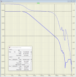
Here's the schematic I drew, and the compensation I ended up with. The CFP triple has lower BW than the EF triple, so I had to increase the compensation. At the same time, low frequency loop gain dropped by 12 dB compared to the 3EF. The 1st Bode plot shows the CFP gain/phase, and the second shows the 3EF gain/phase.
THD at 20 KHz is 49% higher (0.0049% increased 0.0073%) and THD at low frequencies is 9.4% higher (0.00034% increased to 0.00037%). The FC + diamond 3EF is still the preferred design.
I'm going to take these as I get them. I got a little out of order because stinius' change to my anti-sat diodes was easy. Next, I need to show what I found with ojg's proposed change to a CFP triple from the present diamond EF triple.
Here's the schematic I drew, and the compensation I ended up with. The CFP triple has lower BW than the EF triple, so I had to increase the compensation. At the same time, low frequency loop gain dropped by 12 dB compared to the 3EF. The 1st Bode plot shows the CFP gain/phase, and the second shows the 3EF gain/phase.
THD at 20 KHz is 49% higher (0.0049% increased 0.0073%) and THD at low frequencies is 9.4% higher (0.00034% increased to 0.00037%). The FC + diamond 3EF is still the preferred design.
Attachments

Last edited:
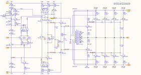
This is the most recent schematic.
Still to be investigated is mcd99's bootstrap compensation technique.
Still to be investigated is mcd99's bootstrap compensation technique.
Attachments

Last edited:
Now, I have some more things to try, wrt compensation. Thank you very much.
Russell,
No problem. Sharing ideas is what it's all about.
Do you have, by any chance, an up to date .asc file? I would like to have a go at stabilizing your design with MIC.
Paul
Last edited:
Hi Paul,
Sounds awesome. That's a time-consuming task, for sure.
Here are the relevant files. Sorry the amp is just a netlist. I have that schematic in Altium.
Change these file names after you download:
Power_Amp_200W.txt --> Power_Amp_200W.net
Power_Amp_200W_asy.txt --> Power_Amp_200W.asy
I believe all the models are included in Power_Amp_200W.net. Most of them are from Bob Cordell's model file, and one or two possibly from Keantoken. I added pin inductance to the power transistors.
Best regards,
Russell
Attachments
This is the most recent schematic.
Some of the currents are mislabeled. I have not been diligent about keeping those updated. For instance, all the predrivers are running about 22mA each at idle.
Russell,
Have started inputting your schematic into ltspice. While doing so had a couple of thoughts.
Could a depletion mode MOSFET be used in place of your floating current source (Q15 and Q16)? Saves a few components.
Could Q30 be referenced to nbias? Saves a GND trace on the PCB? Also a little more symmetrical 😉
Cheers,
Paul
Russell,
Could a depletion mode MOSFET be used in place of your floating current source (Q15 and Q16)? Saves a few components.
I'm not a fan of them. You can do yours that way if you want. I am very happy with the bias leg as it is now.
Could Q30 be referenced to nbias? Saves a GND trace on the PCB? Also a little more symmetrical 😉
Symmetrical how? The only reason Q30 is in the schematic is to equalize the idle Vce of Q5 and Q8, so Q5 does not get so hot. If you don't like the ground trace, just delete Q30, and make sure Q5 has adequate heatsinking for 325 mW dissipation.
The CFP triple has lower BW than the EF triple, so I had to increase the compensation.
That is true, the bandwidth of the EF triple is higher, although in my sim it shows that 30 degree phaseshift appears at 15MHz for both when outputting full negative 56V into 4ohm. So I didn't think the difference in compensation would be that much.
The input impedance of the CFP triple is about 8dB lower than the EF triple, so that probably explains the difference in loopgain at lower frequencies.
Some questions:
Why is your C101 and C102 unequal in the schematic above?
Did you optimize the bias for the CFP triple carefully? If the currents indicated on the schematic is correct it seems quite underbiased. I found that 120mA in the driver and 94mA in the output transistors gave the least THD at 20kHz/20V/4ohm output. The THD goes up quickly with underbiasing, but is quite tolerant to overbiasing.
About the name "CFP triple", I'm not so sure that's what it should be called since it can be confused with the more common CFP configuration where the drivers are also class-B. Maybe "decompensated CFP" or "class-A driver CFP" is better? Neither of them very catchy names, I admit...
Br,
OJG
- Home
- Amplifiers
- Solid State
- RK-Auto200W Amplifer