Hi OJG,
C101 and C102 were actually equal in my sims at 39pF, but I happened to take that snapshot while changing them to 68 pF, for a subsequent sim. Sorry for the circuit typo.
I set the bias in the output transistors at 75mA each, same as in the comparative sim I ran with the EF triple. The EF triple is very tolerant of a fairly wide range of bias currents.
I do not recall the exact current in the driver transistors. I used the same values for Rc and Re that you did there, but my ballast resistors for the finals were larger, so probably the driver bias current is a tad higher. I think it was in the 100 mA range.
You're right about the CFP triple. There are lots of circuits that could describe. Class-A CFP is kind of catchy, but could mislead folks that the whole OPS is class A. I'll leave that one to the marketing department. lol. To really use the CFP, I would need to insert a Tian probe into the current feedback path, and wring it out.
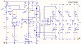
The folded cascode gain is very sensitive to input impedance of the OPS. That is somewhat how I ended up with the OPS configuration that I have. I wish I could get the predriver and driver poles out past 100 MHz, with the final pole at 20 to 30 Mhz. That would let me get the BW that I originally wanted. I may yet play with bias currents at each stage to get more BW for the overall circuit.
Before I posted any circuits, I did a lot of experiments with several stand-alone OPS circuits, including one very like the one you showed. At that time, I was looking for highest BW and highest input impedance. The diamond 3-EF is the only one I actually tried in the full amplifier.
I've been trying lots of experiments lately, to optimize performance. A few have helped incrementally. Most have actually hurt performance. I feel like things are getting close to being dialed in. Paul (mcd99) seems to have some particular insight on compensation, so I'm hopeful that his and my experiments there will yield some performance boost with two-pole compensation. I would still like to meet the goal of <0.001% THD at 200W, 20 kHz.
I had high hopes for the EF+CFP triple (look what I did there). I really thought it might be the answer to getting high OPS linearity.
The experimenting is fun, and there's no marketing department to come in and shoot the engineer and ship the product. Still, I really do want to build some amplifiers, and get a new design for DIY'ers to play with.
C101 and C102 were actually equal in my sims at 39pF, but I happened to take that snapshot while changing them to 68 pF, for a subsequent sim. Sorry for the circuit typo.
I set the bias in the output transistors at 75mA each, same as in the comparative sim I ran with the EF triple. The EF triple is very tolerant of a fairly wide range of bias currents.
I do not recall the exact current in the driver transistors. I used the same values for Rc and Re that you did there, but my ballast resistors for the finals were larger, so probably the driver bias current is a tad higher. I think it was in the 100 mA range.
You're right about the CFP triple. There are lots of circuits that could describe. Class-A CFP is kind of catchy, but could mislead folks that the whole OPS is class A. I'll leave that one to the marketing department. lol. To really use the CFP, I would need to insert a Tian probe into the current feedback path, and wring it out.
The folded cascode gain is very sensitive to input impedance of the OPS. That is somewhat how I ended up with the OPS configuration that I have. I wish I could get the predriver and driver poles out past 100 MHz, with the final pole at 20 to 30 Mhz. That would let me get the BW that I originally wanted. I may yet play with bias currents at each stage to get more BW for the overall circuit.
Before I posted any circuits, I did a lot of experiments with several stand-alone OPS circuits, including one very like the one you showed. At that time, I was looking for highest BW and highest input impedance. The diamond 3-EF is the only one I actually tried in the full amplifier.
I've been trying lots of experiments lately, to optimize performance. A few have helped incrementally. Most have actually hurt performance. I feel like things are getting close to being dialed in. Paul (mcd99) seems to have some particular insight on compensation, so I'm hopeful that his and my experiments there will yield some performance boost with two-pole compensation. I would still like to meet the goal of <0.001% THD at 200W, 20 kHz.
I had high hopes for the EF+CFP triple (look what I did there). I really thought it might be the answer to getting high OPS linearity.
The experimenting is fun, and there's no marketing department to come in and shoot the engineer and ship the product. Still, I really do want to build some amplifiers, and get a new design for DIY'ers to play with.
I've been trying lots of experiments lately, to optimize performance. A few have helped incrementally. Most have actually hurt performance. I feel like things are getting close to being dialed in. Paul (mcd99) seems to have some particular insight on compensation, so I'm hopeful that his and my experiments there will yield some performance boost with two-pole compensation. I would still like to meet the goal of <0.001% THD at 200W, 20 kHz.
I had high hopes for the EF+CFP triple (look what I did there). I really thought it might be the answer to getting high OPS linearity.
So far I have created an ltspice schematic with all your models. Not implemented your bias circuit yet so use Iservo to set the OPS bias. Currently biasing the OPS at 70mA.
Haven't managed to improve performance yet, however, I have managed to get two pole MIC working. Pretty much the same performance as you have with shunt only but with a ULGF of ~1 MHz for the main feedback loop. The loop gain at 20khz was 51dB.
Please disregard my question on the Q30 reference. I was talking rubbish. Also, I am sticking to your design and design choices regarding the depletion mode MOSFET.
Have you seen this thread? It may be of interest...
A three transistor compound pair?
Will update you when I have reached a conclusion on my compensation ideas. It's still early days. Need a little more time and don't want to pollute your thread with excess posts.
Best regards,
Paul
You won't be able to use the auto-bias circuit for regular simulations. It takes over a second to spin up and settle. Even with a preset initial condition, most simulations would just run at the initial condition. 70 mA / output transistor seems to be a good bias level.
Your numbers with TPMIC are similar to what I was getting, also with no net improvement to HF THD. Still, I think your method has promise. I don't have time to look at it for a few days.
On the bias leg: Frankly, for simulations, you could just use a SPICE DC current source in place of the ring-of-two current source. If you have a depletion FET that reliably produces current in the neighborhood of 2 mA, that works well, too.
Interesting thread on three-transistor compound pairs.
Will update you when I have reached a conclusion on my compensation ideas. It's still early days. Need a little more time and don't want to pollute your thread with excess posts.
Paul...
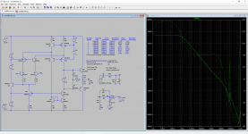
OMG. I'm trying this circuit, and it's still very preliminary. I'm getting these results. This seems like it will be awesome.
ULGF = 3.2 MHz
PM = 60.7 deg
GM = 10.3 dB
LG @ 20 kHz = 61.6 dB
PM = 60.7 deg
GM = 10.3 dB
LG @ 20 kHz = 61.6 dB
Now, the let-down. THD is worse at 20 kHz, and only slightly better for a very small range between 1 kHz and 3 kHz. Bypassing a stage or two of the 3EF lowers the impedance at the FC output. This kills the gain and the linearity correction at high audio frequencies.
I have not given up on this technique, but now that I see how the trade-off mechanisms work, I am less optimistic.
Attachments


Russell,
The best I have achieved so far is 0.002 @ 200W. Not given up yet... I also found the compensation I used with apparent success in my amp doesn't do well for yours. The question is why? I know it's not the OPS as I sustituted my 3EF and the results were slightly worse.
My experience with my FC amp is that the real gains come from having an OPS with gain (eg X3). Found the folded cascode doesn't seem to do well with large voltage swings. This brings mythical THD figures in Sims and a few extra challenges like dealing with clipping. I'm not suggesting you go this way as it doesn't seem to be in the spirit of this amp and adds significant complexity but just my thoughts (and the direction I'm heading in).
It's like the input stage is the limiting factor and not the OPS. At least with my amp I found the performance suggested by the loop gain wasn't fully reflected in trans Sims. This is what lead me to concede to the use of single pole MIC with a little shunt in subsequent designs. Too many compensation loops equals too many chances to make a mistake.
Paul
The loop gain is the limiting factor. The input stage has almost no distortion at all, I have learned in some experiments I have run. Even as differential current increases to charge the compensation, it remains linear with the 22.1 ohm RE.
OTOH, any compensation that reduces the impedance at the FC output node tends to cancel any benefit conferred by that compensation. Likewise, any change in output stage seems to offer less linearity improvement than the gain it is killing in the FC stage.
The bootstrapped compensation greatly reduces the impedance of the FC output stage at high audio frequencies, roughly equal to the extra gain provided by TPIIMC.
Sorry for even more armchair engineering here, but this thread is so interesting that I can't help myself.
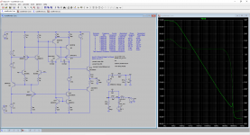
I made a simplified version of your input stage in LTspice, with just a predriver for output stage. I got 0.005% THD at 20k at 56V which matches well your own simulation back in post 114. Which again shows that it is not the output stage that is limiting the THD performance of this amp anymore. I agree with Paul that the FC stage just hasn't got any more to give with these large voltage swings.
Now it struck me when looking at the schematic that by just rearranging two of the transistors, I got a push-pull VAS stage. Compensating this VAS is straightforward and the ULGF, PM and LG@20kHz becomes the same as the FC. The interesting thing is that even though the Bode plot is the same (above 10kHz) now the THD at 20k at 56V is 0.0002%, that's more than an order of magnitude better! Which shows that THD can be reduced in more ways than just by adding more loopgain. Imagine what the number could be when adding two-pole compensation as well! (I'll save you the trouble, it's <1ppm)
I'm not saying you should throw away the FC and go for a push-pull VAS, but that maybe it's time to accept that you got the most from the FC topology and just start building it. I highly recommend splitting input stage and output stage in two PCBs to make it easy to experiment with different architectures later.
Br,
OJG
Attachments

Interesting result, ojg.
I am indeed getting close to pulling the trigger on building the PCB using just output compensation. Charging Ccomp at full swing, 20 kHz likely makes the input pair the limiting factor on THD. That's why I'm still pursuing input-inclusive compensation.
I do plan, after this design is finished, to design a more traditional LTP+VAS amplifier, but probably not with a differential VAS. I suppose it will look like the many different blameless badger wolverine amps here on DIYaudio. I may do the EF+CFP output stage on that amp, just to make it a little unique.
Last edited:
It's not longtime ago, i also have similar result with OJG when i tried to sim a folded cascode design which same to Luxman M-02 - the VAS cascoded to LTP. Can't break <10ppm THD level. I change a bit the design to ordinary push-pull VAS, it's much more better.
The simple reason i see that loop gain is the key of issue.
Regards,
The simple reason i see that loop gain is the key of issue.
Regards,
I think that's right. It needs more loop gain at 20 kHz. With a common-emitter VAS, you have lots more gain, and you can gain the full benefit of 2-pole Miller compensation.
However, I have about 86 dB of loop gain, low frequency. I think if I can keep the differential current low in the LTP, I can keep the distortion in the LTP very low. I still won't have as much gain to correct output stage distortion as I'd like to have, but I the input stage distortion can be very low, relatively.
However, I have about 86 dB of loop gain, low frequency. I think if I can keep the differential current low in the LTP, I can keep the distortion in the LTP very low. I still won't have as much gain to correct output stage distortion as I'd like to have, but I the input stage distortion can be very low, relatively.
Russell what if you combine your FC Design with an samuel grooner stage, maybe you can squeeze the performance even more??
It was also samuel grooner push-pull transimpedance stage i thought about. Look here
A new audio amplifier topology with push-pull transimpedance stage-Part 2 : Biasing , stability and AC performance | Semantic Scholar
A new audio amplifier topology with push-pull transimpedance stage-Part 2 : Biasing , stability and AC performance | Semantic Scholar
Last edited:
Russell what if you combine your FC Design with an samuel grooner stage, maybe you can squeeze the performance even more??
Groner Triple
Thanks, jcarr. I would not have known what Kim was talking about without the link.
That Groner output stage is not much different that what I have now. In fact, I tried it with the collectors bootstrapped that way, and I was not happy with the AC poles and zeroes.. This was early on, when I was looking at just the output stage, before I attached it to the folded FC stage.
I can see that this might offer me some significant advantages to what I have now. In my own experiments, I have determined that the input pair are the source of hardly any of my distortion at high power/high frequency. However, when I simulate the output stage, its distortion is not very high either.
The effect that is left is interaction between the VAS output and the triple EF input, in other words, VAS loading. The bootstrapping of the first EF potentially cures a huge amount of that, and allows me a much higher beta device in that location, with much lower C in general. I'm thinking BC547/557, but I'm open to suggestions. I'm going to revisit the bootstrapping of the first EF stage, which I believe Jonathon suggested to me in the first place, several weeks ago.
One question I have: Does anyone know why Groner used diodes in between the emitters of his center EF stage. That seems counter-intuitive for bias stability of the center EF stage
As far as adding some second folded cascode stage as part of the output stage, no that's too convoluted for my tastes. I'm looking for minimum gain stages.
Hi Russell,
if I remembered correctly, those two are the internal thermal tracking diodes internal to the output transistors, they were put in the 2nd EF circuit to help mitigate the bias control tempco variation over the temperature range.
if I remembered correctly, those two are the internal thermal tracking diodes internal to the output transistors, they were put in the 2nd EF circuit to help mitigate the bias control tempco variation over the temperature range.
If increased global NFB is the preferred path to lower distortion, keeping the impedance of the gain node as high as possible is a top priority.
Bootstrapping the first EF would open the door to a wider range of candidates for Q12 and Q13, including low voltage types (usually high beta implies a thin base, which in turn reduces Vceo).
Would 2SA970 / 2SC2240 improve things? 2SA1016 / 2SC2362? 2SA1587 / 2SC4117?
kind regards, jonathan
Bootstrapping the first EF would open the door to a wider range of candidates for Q12 and Q13, including low voltage types (usually high beta implies a thin base, which in turn reduces Vceo).
Would 2SA970 / 2SC2240 improve things? 2SA1016 / 2SC2362? 2SA1587 / 2SC4117?
kind regards, jonathan
Yep, I definitely see that as the advantage of bootstrapping the 1st EF collectors. Maximizing the impedance at the FC output has been my goal from the beginning.
You give so many Japanese part numbers, lol. I'll look them up. Right now I'm trying BC547/557, which have a beta of 300 in this particular model.
You give so many Japanese part numbers, lol. I'll look them up. Right now I'm trying BC547/557, which have a beta of 300 in this particular model.
- Home
- Amplifiers
- Solid State
- RK-Auto200W Amplifer