Yes, it's flexible, in the non global feedback version, the FB resistor is replaced with a LFB resistor for the input transistors, gain can be easily adjusted by changing this LFB resistor.That does look like a good alternative FE.
The FFT profile can be shaped by altering the R21/R22 resistors, at least in LTspice.
Attachments
That does look like a good alternative FE. Every thing suggests that the FE be on a PCB separate from the OS its bias control circuits, allowing alternate FEs to be paired with the OS.
Yes keeping the Output Board separate and trying different Front Ends makes the most sense. One can achieve system synergy much easier and with less wastage.
I have been playing with the M25 output stage (Mosfets in both rails as published in SissySIT thread, directly driven by an H2 board. My speakers are Fostex FE168Sigma in MLTLs, connected in reverse polarity.
The sound is as good as the Input signal can get. Never heard such an expansive sound stage with height resolution. The timbre and tonality is stunning. Now I am looking at the cascoded Input stage here, a few posts earlier with the obsolete Toshiba mosfets (of which which I have 10 each) and H2 dialed in as per personal preference.
XA25 did come out particularly neat....
🙂
It's a semblance of the kind of thing the XA25 offers. No output stage degeneration, Square law effect, Zero negative feedback and some generous H2.
I finally concur with you Mr. Pass (after 35 years of DIY). You want to listen to all of your music collection (and not analyze sound). Thank you Mr. Pass for your creative explorations and generosity in sharing with us.
Thank you Indra and ZM for Hall chip output stage which gets rid of source resistors and achieves low distortion with zero negative feedback.
Looking forward to a XA25 like Front End, hopefully with H2 adjustment and sufficient voltage swing.
I did simulation of an xa25 type amp that uses irf9610 and irf610 on the gain and output stages. I used this amp to drive Lynn's output stage. As I kept lowering the attenuation resistors I got lower THD. With 100 ohms and 13.1 ohms the THD read 0.0045 percent at 1 watt.
My my ... Ive been away for a few months and look at all that I’ve missed ! Nice work Lynn 😉
... Can’t wait to built Something with my SITs So very much Subscribed !
... Can’t wait to built Something with my SITs So very much Subscribed !
I did simulation of an xa25 type amp that uses irf9610 and irf610 on the gain and output stages. I used this amp to drive Lynn's output stage. As I kept lowering the attenuation resistors I got lower THD. With 100 ohms and 13.1 ohms the THD read 0.0045 percent at 1 watt.
The 9610 is problematic for the mid-band transconductance shift of P
channel IR parts. You might want to use the Harris version, or some other
Toshiba or Fairchild (OnSemi) part.
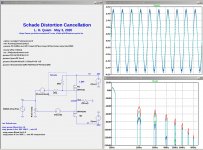
Schade Distortion Cancellation
While working on an explanation for SIT3X distortion cancellation I decided to see if Schade feedback actually behaved like a SIT in the SIT3X circuit. Here are the results using IRFP240 and IRFP9240 FETs. In the 1st image spectral plots, the colors are:
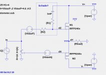
I did some equation pushing and derived the triode parameters of the simple Shade common-source circuit, shown in the 3rd image. It is important to note that μ is the common-source gain factor with a constant current source as a load, and gm[FET] is dependent in the bias current, thus the values of Rdrain and gm[Schade] change with bias current. Plugging these equations into the equations in post #142 SIT measurements, Mu Follower, and amplifier build should provide the cancellation behavior shown in the simulation.
While working on an explanation for SIT3X distortion cancellation I decided to see if Schade feedback actually behaved like a SIT in the SIT3X circuit. Here are the results using IRFP240 and IRFP9240 FETs. In the 1st image spectral plots, the colors are:
- Rload A
- 4R 1 red
- 8R 1 cyan
- 4R .9 green
- 8R .9 blue
I did some equation pushing and derived the triode parameters of the simple Shade common-source circuit, shown in the 3rd image. It is important to note that μ is the common-source gain factor with a constant current source as a load, and gm[FET] is dependent in the bias current, thus the values of Rdrain and gm[Schade] change with bias current. Plugging these equations into the equations in post #142 SIT measurements, Mu Follower, and amplifier build should provide the cancellation behavior shown in the simulation.
Attachments

I am not sure that the circuit shown in Nelson Pass's 2015 Burning Amp video behaves that same as Schade feedback in my previous post (50w Single-Ended BAF2015 Schade Enabled).
I believe that the circuit behaves more like that in the schematic below, which behaves as simple feedback, without a dependency on the DC voltage on the drain.
I believe that the circuit behaves more like that in the schematic below, which behaves as simple feedback, without a dependency on the DC voltage on the drain.
Attachments
Thanks Mr. Pass, I am aware of that, I think I first saw that in one of your articles. I wasn't going to use those mosfets. I used them because the models I have for them are closely matched. I think I got them from an Euvl simulation.
I'm hoping that one of the three auto bias circuits I simulated will work with the more temperature sensitive mosfets. I don't have any Toshiba's but maybe Exicon would work. The Onsemi are easy to find and fairly easy to match so I will try those first. However, I didn't like the models I found for them.
I'm hoping that one of the three auto bias circuits I simulated will work with the more temperature sensitive mosfets. I don't have any Toshiba's but maybe Exicon would work. The Onsemi are easy to find and fairly easy to match so I will try those first. However, I didn't like the models I found for them.
Is the chapter on the SIT output stage closed already, or are there some hardware measurements to be made? I would really like to build this.
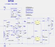
SIT3X Output Stage Status
The SIT3X output stage is "mostly" complete. Here are some remaining issues:
The SIT3X output stage is "mostly" complete. Here are some remaining issues:
- Bias Circuit: I want to test 2nd generation XA25 opto bias circuit , which use zeners and has lower valued sense resistors. That bias circuit has some other properties that are desirable.
- Power Supplies:
- PS ground at V+ rail: V(V+)=0, V(V-)=-94V. This variant does not require the capacitance multiplier, but does require separate supplies for the FE.
- PS Ground at FE ground: V(V+)=47V, V(V-)=-47V. This variant requires the capacitance multiplier on V+, or other means to reduce V= ripple.
- Front End: Several alternatives, including two or more with with zero global feedback.
Attachments

Correction to the previous post. It should have been:
"My personal inclination is to go for V(V+)=+47V, cap multiplier, folded-cascode FE, and 2nd gen XA25 opto bias."
That s the configuration I've been most interested in as well. I will be inclined to make some of the part substitutions I mentioned in the folded cascode front end. I have a couple different cap multiplier designs that I'm already working with.
Basic PSU would start with an Antek AN-10435, which has four 35V secondaries. I have a set of Prasi's CRC boards with the LT4320 based rectifiers. These can accept a cap multiplier in between the bulk supply caps, or not, as needed.
The UMS spec isn't a consideration for me, as the chassis I want to use doesn't have those holes drilled in the heatsinks. In fact, I can't think of a chassis that supports the necessary power dissipation and also has the UMS hole pattern. I've become pretty adept at drilling and tapping.
Thanks Mr. Pass, I am aware of that, I think I first saw that in one of your articles. I wasn't going to use those mosfets. I used them because the models I have for them are closely matched.
Not a big deal - they might even sound better.... 😉
The Toshiba J313 and K2013 would be my choice, but I also get good
results with the Fairchild/Onsemi FQP3N30 and 3P20, and they are cheap
and available.
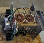
Here is the latest iteration on the output stage. It appears to do well on all of the tests: distortion, AC response, PSSR, and power-up/down "thumps".
After carefully looking at the datasheet for the IXYS depletion mode FET previously used in the cap. multiplier, I discovered that there were issues with the SOA (safe operating area) w.r.t. Rdson. Thus, using a depletion mode FET in the cap. multiplier would not end up reducing the voltage drop. Does anyone have a simple cap. multiplier with a lower voltage drop than shown below?
After carefully looking at the datasheet for the IXYS depletion mode FET previously used in the cap. multiplier, I discovered that there were issues with the SOA (safe operating area) w.r.t. Rdson. Thus, using a depletion mode FET in the cap. multiplier would not end up reducing the voltage drop. Does anyone have a simple cap. multiplier with a lower voltage drop than shown below?
Attachments
Is the chapter on the SIT output stage closed already, or are there some hardware measurements to be made? I would really like to build this.
I am also getting impatient with myself.
 Here is the plan. There will be a new thread for the build. Although I have been calling the output stage the SIT3X, I haven't yet decided on the final name for this amplifier. I will clean up the schematic with rational partitioning and part numbers. Ultimately there needs to be a BOM, and PCB layout(s). Different folks might choose to do different PCB layouts to accommodate their packaging requirements.
I have been working on a variation of a low dropout capacitance multiplier based on one used by Mr Evil. It is not a simple as the "easy cap multiplier," but it has very low dropout by virtue of using a low RdsOn P-channel Mosfet.
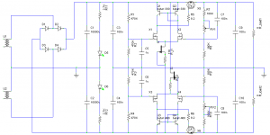
Schematic is the positive portion of the attachment.
For the SIT3X output stage, some adjustments can be made:
R1 and R2 are 22k. C5 is 100 uF, preferably a low impedance organic polymer.
Q1 and Q2 are KSA992, grade F. X1 and X2 are ZVP3310A.
J1 can be a simple CRD such as E-562, taken to ground instead of the negative rail.
X5 is a IXTH52P10. R5 should probably be 47 Ohms.
R7 is 100k, RV1 is 100k, R8 is 220k.
C9 is 100 uF, same as C5. Add 4700 uF to 10,000 uF as needed for energy storage.
A protection diode should be added from the Drain to Source of X5. Probably 1N4003.
Attachments
Last edited:
I am not sure that the circuit shown in Nelson Pass's 2015 Burning Amp video behaves that same as Schade feedback in my previous post (50w Single-Ended BAF2015 Schade Enabled).
I believe that the circuit behaves more like that in the schematic below, which behaves as simple feedback, without a dependency on the DC voltage on the drain.
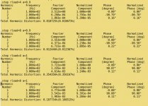
Cancel post #209. I found an error in my simulation FFT and fourier results. In LTSpice I forgot to turn off data compression. I now get identical results to the circuit without the capacitor, except for a DC offset at the input. Both circuits provide harmonic cancellation with proper adjustment of the potentiometer.
- Home
- Amplifiers
- Pass Labs
- SIT measurements, Mu Follower, and amplifier build