Thanks ivanlukic, I will try an output inductor during my experiments. Currently I'm tracking down the source(s) of audible distortion, which is especially noticeable on the board with speaker protection.
Interestingly the protection led glows faint red in time with the music and the distortion is worse on this amp, as though the protection is cutting in and out. I have verified that the offset at the speaker output is in the very low double digit mV range.
When I first built the second board I installed a wire link in place of the input capacitor but couldn't maintain 0VDC at the input under all conditions. I've tested the source - a Sony MP3 portable player and no DC offset is present. My theory is that the input transistor somehow reacts to the source impedance that is present and that shifts the DC offset point as a result. It's a non-issue with C1 in place.
I've been studying this topology and comparing it with the descriptions in Bob Cordell's book. It strikes me as odd that Bigun has chosen to use a trimpot to set the DC offset while an op-amp based DC servo could do the same thing without requiring adjustment and could track 0.00V under all conditions.
Last edited:
Member
Joined 2009
Paid Member
It's hard to resist posting photos
Please post photos !
Interestingly the protection led glows faint red in time with the music and the distortion is worse on this amp, as though the protection is cutting in and out.
I suspect your lower rail voltage prevents enough current flow through the opto-isolator to turn on the MOSFET 'relay' properly. Be careful you don't damage the MOSFETs - they should normally be either ON (low resistance and low dissipation) or OFF (low current so also low dissipation) but if operating somewhere in-between (power dissipated) for any length of time they will heat up. The issue could be one of two places, i) R38 is too high and needs to be reduced (just try another 5k1 in parallel) and ii) Q17 isn't turning on properly because the zener at D5 is too close to the rail voltage (Q17 turns on when the rail voltage is a volt or more above the zener breakdown voltage).
I've been studying this topology and comparing it with the descriptions in Bob Cordell's book. It strikes me as odd that Bigun has chosen to use a trimpot to set the DC offset while an op-amp based DC servo could do the same thing without requiring adjustment and could track 0.00V under all conditions.
I have built a circuit very similar to TGM8 before with a simple servo. It was TGM3 (there's a thread on it around here somewhere). In that design I made a DC servo using a single transistor and it worked OK but produced some delayed turn-on noises - a servo needs to have a long time constant. Bob does say you have to design a servo well to avoid impacting the sound. I thought the present arrangement might have some benefits. But if we wanted, we could readily re-spin the design with a servo. I have another design for a single transistor servo that I prefer to that which I used in TGM3 - too many ideas and too little time !
Progress - I've been adding parts to my first pcb today. It's coming along well. However, I found that I have some wrong parts in my order. The BOM I used doesn't have R41 (I substituted a 27k resistor) or R42,43,44&47 which are only there to 'drain' the rail capacitors when there are no other paths for the current to leak away so I left them off. I also ordered a regular electrolytic for C16 when I should have ordered a bipolar device. And my C15&18 were also ordered wrong, their diameter is bigger than I designed for so not sure if I can fit them yet. Clearly I was in a bit of a rush but nothing bad enough to prevent me building a first channel. I am going to jump ahead and build with the enhanced VAS since you have already shown the basic design functions 😀
Last edited:
Member
Joined 2009
Paid Member
Here's a quick no-flash photo of work in progress.
You can see the two large orangish caps - they aren't soldered in yet, but are over-sized and very close to the TO-126 transistors. But they do just fit and it might work if the transistors don't get hot.
You can see the two large orangish caps - they aren't soldered in yet, but are over-sized and very close to the TO-126 transistors. But they do just fit and it might work if the transistors don't get hot.
Attachments
Bigun said:I suspect your lower rail voltage prevents enough current flow through the opto-isolator to turn on the MOSFET 'relay' properly. Be careful you don't damage the MOSFETs - they should normally be either ON (low resistance and low dissipation) or OFF (low current so also low dissipation) but if operating somewhere in-between (power dissipated) for any length of time they will heat up. The issue could be one of two places, i) R38 is too high and needs to be reduced (just try another 5k1 in parallel) and ii) Q17 isn't turning on properly because the zener at D5 is too close to the rail voltage (Q17 turns on when the rail voltage is a volt or more above the zener breakdown voltage).
I thought the same thing and kept an eye on the FETs to ensure they didn't overheat. At all times they remained cool to the touch, which I found interesting.
I tried reducing R38 from 5k1 to 3k9 but it didn't seem to make any difference.
Tempting fate I installed a 30V zener into D5 since it was the lowest SMT value I had (25V would have been ideal and I'm kicking myself for not ordering some because they are difficult to get locally).
Anyhow I think the problem is the zener so today I swapped in a higher voltage/wattage transformer to see if it fixed the problem.
It did.
This trusty transformer gives me a rock solid 41V at idle and 40V under load with my mains..... putting the BD1xx devices right in their sweet spot 😀
The flickering red light has gone completely and the sound quality has improved 10 fold. The bass is punchy and authorative with the 10uF bipolar input cap; more so than the P3A in my living room, which has a 1uF WIMA film input cap.
I will continue my experiments with low voltage supplies once I have a supply of SMT zeners and resistors on hand.
With the gross distortion eliminated, I can hear some high frequency artefacts that could be distortion, could originate from the power supply (I did go to some efforts with cable routing/twisting on my test rig), or could be coming from the cheap Sony MP3 Walkman.
Tomorrow I'll rule out the usual suspects and then experiment removing C1 an changing the compensation cap values.
[/QUOTE]
Bigun said:I have built a circuit very similar to TGM8 before with a simple servo. It was TGM3 (there's a thread on it around here somewhere). In that design I made a DC servo using a single transistor and it worked OK but produced some delayed turn-on noises - a servo needs to have a long time constant. Bob does say you have to design a servo well to avoid impacting the sound. I thought the present arrangement might have some benefits. But if we wanted, we could readily re-spin the design with a servo. I have another design for a single transistor servo that I prefer to that which I used in TGM3 - too many ideas and too little time !
Is the turn on noise an issue if you have a speaker protection / delayed turn on circuit?
Bigun said:Progress - I've been adding parts to my first pcb today. It's coming along well. However, I found that I have some wrong parts in my order. The BOM I used doesn't have R41 (I substituted a 27k resistor) or R42,43,44&47 which are only there to 'drain' the rail capacitors when there are no other paths for the current to leak away so I left them off. I also ordered a regular electrolytic for C16 when I should have ordered a bipolar device. And my C15&18 were also ordered wrong, their diameter is bigger than I designed for so not sure if I can fit them yet. Clearly I was in a bit of a rush but nothing bad enough to prevent me building a first channel. I am going to jump ahead and build with the enhanced VAS since you have already shown the basic design functions 😀
Sorry Gareth, C16 was incorrectly specified in my original BOM, which I rectified in the December 16 update, after I realised having received the incorrect part in my order.
For some reason R41+ are not in my BOM. I noticed this too when I assembled my first board, but I didn't worry much, especially since I wasn't adding onboard filter caps. When I built the second board I substituted a 8.25k for R41. I'll rectify the BOM soon.
What did you order for C15 & C18? I used Nichicon HE 100uF here (the same part for C8 & C9 also) and had no problems. Please let me know if there are any BOM changes required.
Member
Joined 2009
Paid Member
Hi Ranchu,
Great progress !
So, I still think some optimization of the dc protection will be of benefit but good to hear you have it working good enough. If it does have issues it will be at the low frequencies, where false-triggering could occur.
For me, the things that have affected treble most in an amplifier (except for source & speakers) is the compensation (output inductor and zobel are part of this). But I know some folk have found it important to allow an amplifier to burn-in for many hours. I have not had any experience with noise from power supplies but have had issues with poor wire dress. And of course pcb layout can cause trouble (and we know who to blame for that !!!).
BOM - it's a work in progress based on what I have mis-ordered, my junk box and circuit changes we have found necessary; the quick list of changes from my rough notes:
C15&18 - I bought, by mistake (trying to optimize), high quality Nichicon fine gold 493-10876-1-ND which are a bit too big. If building again (for less than 50V rails) I would specify 493-10919-1-ND as the high-end option. Anyhow, being that the fine gold are so nice I decided to use them for C8 & C9 as I think they will provide the most benefit in these locations. C9 is the bootstrap for the VAS and C8 is the rail cap that the VAS current uses as a return path to ground. For C15&18 I'll probably shoe-horn in the caps that I bought for C8&9 (493-3195-ND) even though they are too large as they are also Nichicon muse and are the 'last caps' in the supply rails so are the caps nearest the output.
For Q4&7 - I went straight for the higher voltage devices, but ended up with KSA1381ESTU-ND (as equivalent to the other high power options we identified) and for Q5&6 with KSC3503DSTFS-ND - I think they are all much the same.
My D5 is 30V so I have some flexibility to use lower rails - I have a nice transformer for 42V good for a stereo although this is lower than my design target of 50V rails.
C16 - I will use a temporary solution and replace it later.
C21,22,21&24 - for use with 42V rails I found some nicely priced CDE caps 338-1626-ND
R41 - I found some 10k parts in my junk box.
R42,43,44&47 - I found some 15k parts in my junk box
R37 - I used P560KFCT-ND as the one on my BOM was out of stock
For some kind of simple economy I made all of R11, R15 and R38 the same 4k7 resistor although I'm not sure if this was wise!
That's it so far....
p.s. thanks for you help, you have made the whole project much more pleasurable by being a great partner for this experiment!
Last edited:
Member
Joined 2009
Paid Member
R38 literally takes some of the 'heat' off from Q17 so at higher rail voltages it helps prevent Q17 from warming up too much. As long as R38 is small enough it isn't critical but I was worried it might have been too large for low rail voltages - seems that wasn't a concern.I tried reducing R38 from 5k1 to 3k9 but it didn't seem to make any difference.
Yes, the delayed turn on should help, but in my TGM3 I didn't have such a circuit. There would be a turn on bump when powered up and then a few seconds later (remember that dc-servo has to have long integration time) the cone would go through a little dance with fairly large excursion. Anyhow I don't think I need a servo with TM8 (TGM9 may be a different story).Is the turn on noise an issue if you have a speaker protection / delayed turn on circuit?
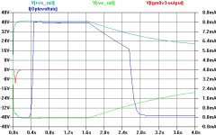
If you want to see how the TGM8 circuit works in sims, see the attached plot. You can see the power rails coming up - the light blue and light green lines (42V version). They reach peak voltage after around 0.2s. After 100 mains cycles the power is off and the rails discharge with a long nearly-exponential decay.
The dark blue trace is the current flow through the optovoltaic that powers the solid state relay. With delayed turn-on provided by R36 + C20 it turns on around 0.47s.
The red trace is the output. Notice the turn-on spike (negative going) and how the solid state relay will keep the output disconnected until the output has settled. There is another 'blip' in the simulated output around 6 s later.
When the power turns off and the rails start to collapse the opto current declines too, also a kind of exponential decay. But then around 2.5s or so the +ve rail voltage drops too low for the breakdown voltage of the zener D5, and Q17 turns off. The opto current declines rapidly and cuts off the output.
I've never seen an implementation like this so I'm feeling like an inventor (just have to make sure it works!) 😀
Attachments
Last edited:
Thinking ahead to parts choice when I come time to build the 50V MOSFET+BJT output version, I've also been toying with the idea of using KSA1381-E, which is specified for the VAS in the VSSA and derivative projects here.
I experimented with a P3A that used MJE15xxx devices and thought the BD1xx sounded better in an otherwise identical setup. It wasn't a small difference either. Mind you I used *either* the MJE or the BD devices "everywhere". My research here and studying the data sheets of these families has led me to believe the MJE15xxx, while well suited as a high power driver is not a good choice for the VAS, which requires high fT and low Cob.
They supposedly work very well for VAS duty (high fT, low Cob) and are used in the VSSA and derivatives.
So my current plan is to use the KSA1381-E for the VAS, its NPN compliment for the bias transistor (it also works well here with a high hfe) and then use the MJE15034/35 as drivers.
Input and compensation cap experimentation...
It was a 35C day here in Brisbane today so we decided to spend a lazy Sunday around the house for the most part. Instead of luxuriating in the air conditioning, I ventured into the hot workshop to spend a few hours quality time with TGM8 😱
Input cap
I thought a wire link would yield the best sound quality but that wasn't to be the case. When I replaced the bipolar I observed around 150-200mA DC offset at the speaker output, which was eliminated whenever an input cap was present. I tried three sources, none of which have any DC offset, and all of which measured resulted in more-or-less the same offset when connected to TGM8.
Although the music played fine with the wire link, there was always a faint but noticeable hiss and other high frequency artefacts present that were largely eliminated with the input cap.
I also experimented with a 1uF WIMA and 2.2uF EPCOS film caps. I expected the bass would be diminished in comparison to the with the 10uF bipolar. But again I was surprised: the bass response seemed the same, but with perhaps a slight audible reduction with the 1uF. Overall the difference between these two film caps was virtually indistinguishable: there is no way I could pick between them in a blind comparison.
That said, my overall impression is that the sound across the entire frequency range seemed a little "thinner" with the film caps. The bipolar gave up nothing in terms of clarity or detail.
I'm a little surprised but for me the winner is the 10uF Nichicon Muse bipolar.
Compensation caps
Both boards were built with a 100p miller cap and 33p phase lead compensation cap. The biggest improvement so far has been from tweaking the miller cap (C4). The 100p was exchanged with 82p, 68p, 56p in turn. 68p was a noticeable improvement over 100p, but the 56p didn't sound any "better" than 68p so I decided not to tempt fate and left it at 68p. I kept an eye on transistor temps and everything stayed cool to warm after an hour of music so I'm fairly confident of adequate stability margin.
Next I played with the lead comp cap by reducing it from 33p to 22p. Here the difference was not really noticeable. It was stable with 22p so I left it at that.
Member
Joined 2009
Paid Member
Wow, a goldmine of information !
Input cap - the dc-offset will be partly determined by the base current into Q1 (itself about 1/100th of the current through it's collector). It flows through R2 to produce a voltage drop of roughly 6uA x 27k = 162mV. When you take the input cap away the base current is provided by your relatively low impedance source and this voltage drop goes away and the output dc-offset changes as you observe; it should be adjustable back to zero using VR1. I didn't think about this source-dependence so I'm glad I followed everyone's advice to include an input cap in the end.
Very interesting report on the effect of the capacitor on the sound, it confirms some of what was said back in post #80, very interesting indeed.
You did a great job with the compensation. I never wouldh've believed it myself but Hugh asked me to try the same experiment with my very first amp, TGM, and I found there was a sweet spot for Cdom. Too big and the sound became less exciting, too small and it became tizzy - but that was with an LTP input though. Some folk say the Singleton input requires less Cdom than an LTP and so is 'better', but the real proof is in the sound, as you have found out. You are at the point though, where a 'scope would help reveal more details of the stability based on the 'traditional' square wave testing (an interesting caution here though: http://www.angelfire.com/ab3/mjramp/sw.html) although you have to be careful not to over-stress the amplifier with high frequency square waves as you can blow it up very quickly.
fyi - in recent simulations I believe for the enhanced VAS that R7 could be higher (4k7) to gain a couple of degrees more phase margin.
Last edited:

Member
Joined 2009
Paid Member
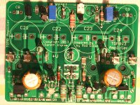
More progress. I've completed assembly as far as having the power BJTs mounted on the heatsink. Not installed are the big rail caps or the MOSFETs. It's a tight layout, some of the parts will be very hard to remove if I blow them up...
I found a cap to use for C16, robbed off my TGM7. And for C15&18 I went with the over-sized caps as I couldn't find any alternatives in my junk box.
The LED is out of focus in these images because I installed it with the leads still long and the LED sitting up high above the board. This is temporary, it's to make it easier to remove it if later I want to move it off-board, say to the front panel.
Attachments
Last edited:
Hi Bigun, thanks for your kind words and encouragement; it is quite exciting to experiment with this design. Your board is coming along nicely, and at this rate it should be ready in time for Christmas (2014) 😀
I know what you mean about it being tight, particularly on the flip side where some of the components are partially obscured by the primary output devices. I had to carefully pry back mine to access the components underneath. But I wouldn't want to do that more than once or twice otherwise the leads will snap off in my experience. Maybe leave off the secondary pair of outputs until you have verified operation and conducted some preliminary analysis?
I'm kinda in a holding pattern until you have finished your board and able to report on the results of the two pole VAS and power FET arrangement, and if it gets the green light, provide some updated component values. Without a scope I can only make qualitative "seat of the pants" assessments, so I don't want to stray too far from the original P3A design that I know well.
Which is basically just a long winded way of saying "hurry up I want to start on my third board but you are holding me up" 😉
Member
Joined 2009
Paid Member
he he he... patience now...well I have made some progress...
Yes, you have to build this board in a certain order. I completed my first board, leaving off the MOSFETs and C10, both are relatively easy to add later.
My bench supply goes to +/-20V and using this I powered it up fine. I then found another old supply and wired up the two supplies together to allow me to go to +/-41V and still with some overcurrent protection.
I found I could set dc-offset to a few mV with bias set to 19mV across the 0R33 resistors - it was stable for 15 minutes but the heatsink was still cool.
The voltage at Q1 emitter was -0.8V, a good match to simulation of -0.8V
The voltage at Q2 emitter was -5.6V, also a good match to simulation of -5.7V
The voltage at Q15 emitter was +1.3V, a bad match to simulation of +2.9V
On cycling the power I could see the LED flash red - as expected since it should start-up with the SS relay 'open' and then close after about half a second.
I found two issues:
1) the silk screen is wrong, 'offset' and 'bias' which were printed near VR2 and VR1 to make it easier to set it up are transposed. Dissapointing to make such a silly error.
2) the circuit design is wrong with regards the LED, preventing it glowing green when the SS relay is 'closed'. I missed it in the simulation because I used a regular LED in place of the Opto. The opto has a much smaller voltage drop - it's in the datasheet but I missed it. As a result, there isn't enough voltage to light up the green LED. I am exploring 3 possible options to fix this.
Last edited:
Thanks for the update Bigun... I'm excited to hear you've got your first board up and running now.
1) I didn't even notice the silkscreen writing to be honest. Looking at the board now I see what you mean but I doubt anyone would really notice unless you pointed it out. An easy fix for MkII.
2) I can confirm mine flashes red momentarily on start up but never turns green. I was wondering why it isn't 'green', was going to enquire with you about that, suspecting a small error in the schematic.
Member
Joined 2009
Paid Member
Hi,
Well more progress.
Compensation: I'm using 22pF for C5 lag, 330pF for C6, 22pF for C4, 4k7 for R7, 100pF for C11, nothing yet for C10.
There isn't an easy fix for the LED without surgery. It's an easy fix if I re-spin the pcb but I'm not sure it's worth it unless there are other things worth changing. There are two options i) Insert a resistor in series with the opto isolator so that there is a higher voltage at the emitter of Q15, sufficient for the green LED. Simple fix but would need surgery on the current pcb. OR ii) take the grounded side of R39 to a -ve voltage instead. Again, this requires a new pcb or you could remove R39 from the board and then run a fly-wire from the common cathode on the back of the pcb with a series through-hole 82k resistor to the -ve rail. It can be done and it would be out of sight but I don't like it - feels messy.
What I did was to take the LED off the board, figuring that it would be nice to mount it on the front panel as an indicator. I took a piece of dual-core wire and soldered it to the pcb where the LED normally goes and put the LED on the end of the wire - I used two-core wire and didn't connect the common cathode. Using a separate wire I connected the common cathode of the LED to the -ve power rail via an 82k resistor. This makes it work fine. Now you turn it on, get a flash of red and then green. It stays green whilst running.
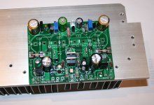
I installed the MOSFETs. Not so easy because you need to ensure all 4 power devices will lie flat on the heatsink - I kind of botched it in there but I think there is a smart way to do this using a small jig (flat piece of material, holes to match the mounting holes and all the devices bolted through it and the pcb) in order to hold all the devices parallel before you solder them in. I strongly recommend you do that and don't do it by hand-eye coordination like I did.
On powering back up, the dc-offset had drifted by around -30mV. It took me a couple of minutes to realize I had forgotten to plug in the input connector which is where the signal ground finds it's way back to the power supply ground. After plugging in the connector the dc offset returned close to zero.
I soldered a short length of miniature coax to the input and put an RCA socket on the other end. I plugged in an RCA cable to allow me to feed signals to the amplifier.
Oscilloscope: I hooked up the scope to the output and grounded the input. I saw random noise on the output, I measured it at around 20mV p-p. I don't know if this is good or bad but this is on the bench with wires all over the place.
With no load I connected the input to the square wave output on the front of the scope (it's a 0.5V p-p 1kHz square wave with 50% duty cycle for calibrating scope probes) and observed a very clean square wave on the output. The output had an amplitude of around 15V p-p which is a gain of 30. Which is within 10% of what you'd calculate for the amplifier (and within the error margin of my rough measurement).
I then wired the output through an inductor to a speaker binder posts and then wired up an 7.8 Ohm dummy resistive load to the binding posts. I re-applied the square wave and immediately had to increase the current limit of the power supply. Square wave was clean, slight rounding of the corners with no ripple or overshoot (haven't tried adding capacitive load yet). Power supply was sourcing around 1/2 Amp per rail which is about right. I didn't run the square wave for long - nervous about causing some damage, nothing got hot.
I decided to try a real speaker, so I wired one up. When I turned on the power there was a small 'bump' from the speaker and the LED was red. I found -40V on the output (before the SS relay, which was doing it's job and cutting off the speaker from the dc at the output - it Works !). However, it means I've managed to blow up the amplifier somewhere. Nothing hot, no smoke and very little current draw.
I was so hoping to hear some music, but I think it's time to call it a night and find out what I've destroyed tomorrow. Not sure what I did wrong, I suspect I turned on the power asymmetrically, one rail before the other, but don't expect this would have caused damage.
Well more progress.
Compensation: I'm using 22pF for C5 lag, 330pF for C6, 22pF for C4, 4k7 for R7, 100pF for C11, nothing yet for C10.
There isn't an easy fix for the LED without surgery. It's an easy fix if I re-spin the pcb but I'm not sure it's worth it unless there are other things worth changing. There are two options i) Insert a resistor in series with the opto isolator so that there is a higher voltage at the emitter of Q15, sufficient for the green LED. Simple fix but would need surgery on the current pcb. OR ii) take the grounded side of R39 to a -ve voltage instead. Again, this requires a new pcb or you could remove R39 from the board and then run a fly-wire from the common cathode on the back of the pcb with a series through-hole 82k resistor to the -ve rail. It can be done and it would be out of sight but I don't like it - feels messy.
What I did was to take the LED off the board, figuring that it would be nice to mount it on the front panel as an indicator. I took a piece of dual-core wire and soldered it to the pcb where the LED normally goes and put the LED on the end of the wire - I used two-core wire and didn't connect the common cathode. Using a separate wire I connected the common cathode of the LED to the -ve power rail via an 82k resistor. This makes it work fine. Now you turn it on, get a flash of red and then green. It stays green whilst running.
I installed the MOSFETs. Not so easy because you need to ensure all 4 power devices will lie flat on the heatsink - I kind of botched it in there but I think there is a smart way to do this using a small jig (flat piece of material, holes to match the mounting holes and all the devices bolted through it and the pcb) in order to hold all the devices parallel before you solder them in. I strongly recommend you do that and don't do it by hand-eye coordination like I did.
On powering back up, the dc-offset had drifted by around -30mV. It took me a couple of minutes to realize I had forgotten to plug in the input connector which is where the signal ground finds it's way back to the power supply ground. After plugging in the connector the dc offset returned close to zero.
I soldered a short length of miniature coax to the input and put an RCA socket on the other end. I plugged in an RCA cable to allow me to feed signals to the amplifier.
Oscilloscope: I hooked up the scope to the output and grounded the input. I saw random noise on the output, I measured it at around 20mV p-p. I don't know if this is good or bad but this is on the bench with wires all over the place.
With no load I connected the input to the square wave output on the front of the scope (it's a 0.5V p-p 1kHz square wave with 50% duty cycle for calibrating scope probes) and observed a very clean square wave on the output. The output had an amplitude of around 15V p-p which is a gain of 30. Which is within 10% of what you'd calculate for the amplifier (and within the error margin of my rough measurement).
I then wired the output through an inductor to a speaker binder posts and then wired up an 7.8 Ohm dummy resistive load to the binding posts. I re-applied the square wave and immediately had to increase the current limit of the power supply. Square wave was clean, slight rounding of the corners with no ripple or overshoot (haven't tried adding capacitive load yet). Power supply was sourcing around 1/2 Amp per rail which is about right. I didn't run the square wave for long - nervous about causing some damage, nothing got hot.
I decided to try a real speaker, so I wired one up. When I turned on the power there was a small 'bump' from the speaker and the LED was red. I found -40V on the output (before the SS relay, which was doing it's job and cutting off the speaker from the dc at the output - it Works !). However, it means I've managed to blow up the amplifier somewhere. Nothing hot, no smoke and very little current draw.
I was so hoping to hear some music, but I think it's time to call it a night and find out what I've destroyed tomorrow. Not sure what I did wrong, I suspect I turned on the power asymmetrically, one rail before the other, but don't expect this would have caused damage.
Last edited:
Member
Joined 2009
Paid Member
More progress...
I chased down the issue to R18 - it was blown. No physical signs of damage but it measured over 300k instead of 100R. The only thing I can think of is that I inadvertently shorted the output to the -ve rail and pulled a large current through the VAS. I replaced R18 with a 560R resistor in order to improve PSRR on the +ve rail. Powered up without issue, LED green. Had to reset dc offset due to change in R18 value. I tried to simulate the amp with a blown R18 but it didn't produce the same voltages at Q1 and Q4 that I measured before I fixed it - don't know why.
Decided to try some music whilst it was working. After having demonstrated the dc-protection works I was good to hook up my B&W floorstander. Input via ipod, MP3 I'm afraid. However, I did not find anything to complain about. Treble was clean and extended, bass was also deep. I didn't detect any sibilance (which I hate). Overall my first impression was 'refined & dynamic' - if I had a volume pot handy I would have brought my CD player into action. I wasn't able to push it though, it was already pretty loud and the panel meter on the power supply hardly reached into the 100mA (average) range. After listening for half an hour I was left wanting more.
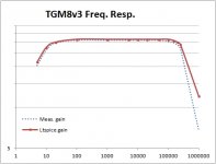
I hooked up a sine wave generator and 7.8R dummy load to measure the frequency response. My sine wave generator is refurbished, it has some nasty artifacts at the peaks of the waveform at high frequencies but otherwise does the job well. The measured results, compared with the simulated freq. response is attached.
At high frequencies I saw some signs of trouble - I could not take reliable data in the range 300kHz to 500kHz without exciting the amplifier into wanting to draw a lot of current. I don't know why this was - didn't have time today to chase it down. Could be a wiring related oscillation (wires all over the bench) or it could be design related. There was no sign of any high frequency oscillations riding as parasitics on the signal, the sine wave looked very clean and the zobel remained cool. I also don't know how well behaved the power supplies are, the +ve rail is a modern unit, the -ve rail was a unit recovered from the e-waste and looks old. They are both regulated. I fitted 100pF for C10 but this didn't make any noticeable difference.
I tried to heat up the dummy load but I didn't get past luke warm. I found the amplifier heatsink was getting pretty hot by the time I was running a continuous 1kHz sine wave at 20V p-p. The +ve rail was drawing on average 440mA. There were no signs of any bias instability. I measured the idle current whilst the amp was hot, it was around 23mV/0.33R, about 15% higher than cold. The drivers were only warm (although they got warmer when running at 100kHz+); the VAS remained cool.
I'm not comfortable with how hot the output power BJTs got, but I didn't find anything wrong otherwise.
I chased down the issue to R18 - it was blown. No physical signs of damage but it measured over 300k instead of 100R. The only thing I can think of is that I inadvertently shorted the output to the -ve rail and pulled a large current through the VAS. I replaced R18 with a 560R resistor in order to improve PSRR on the +ve rail. Powered up without issue, LED green. Had to reset dc offset due to change in R18 value. I tried to simulate the amp with a blown R18 but it didn't produce the same voltages at Q1 and Q4 that I measured before I fixed it - don't know why.
Decided to try some music whilst it was working. After having demonstrated the dc-protection works I was good to hook up my B&W floorstander. Input via ipod, MP3 I'm afraid. However, I did not find anything to complain about. Treble was clean and extended, bass was also deep. I didn't detect any sibilance (which I hate). Overall my first impression was 'refined & dynamic' - if I had a volume pot handy I would have brought my CD player into action. I wasn't able to push it though, it was already pretty loud and the panel meter on the power supply hardly reached into the 100mA (average) range. After listening for half an hour I was left wanting more.
I hooked up a sine wave generator and 7.8R dummy load to measure the frequency response. My sine wave generator is refurbished, it has some nasty artifacts at the peaks of the waveform at high frequencies but otherwise does the job well. The measured results, compared with the simulated freq. response is attached.
At high frequencies I saw some signs of trouble - I could not take reliable data in the range 300kHz to 500kHz without exciting the amplifier into wanting to draw a lot of current. I don't know why this was - didn't have time today to chase it down. Could be a wiring related oscillation (wires all over the bench) or it could be design related. There was no sign of any high frequency oscillations riding as parasitics on the signal, the sine wave looked very clean and the zobel remained cool. I also don't know how well behaved the power supplies are, the +ve rail is a modern unit, the -ve rail was a unit recovered from the e-waste and looks old. They are both regulated. I fitted 100pF for C10 but this didn't make any noticeable difference.
I tried to heat up the dummy load but I didn't get past luke warm. I found the amplifier heatsink was getting pretty hot by the time I was running a continuous 1kHz sine wave at 20V p-p. The +ve rail was drawing on average 440mA. There were no signs of any bias instability. I measured the idle current whilst the amp was hot, it was around 23mV/0.33R, about 15% higher than cold. The drivers were only warm (although they got warmer when running at 100kHz+); the VAS remained cool.
I'm not comfortable with how hot the output power BJTs got, but I didn't find anything wrong otherwise.
Attachments
Last edited:
Very interesting Bigun... thanks for the detailed write-up. Do you plan to run some tests with simple VAS compensation, or are you satisfied that the 2-pole scheme is better and the other not worth pursuing further?
Have you modelled or measured the degree of current sharing is between the BJTs and MOSFETs, at various signal amplitudes? You said earlier in this thread that the FETs start to conduct only after a certain minimum threshold, and I think it was ASKA who made the observation that the MOSFETs will saturate before the BJTs. If the signal voltage increases above the threshold where the MOSFET saturates, then additional current drive will need to be met solely by the BJTs as the output continues to rise (approaching the rails).
Have you modelled or measured the degree of current sharing is between the BJTs and MOSFETs, at various signal amplitudes? You said earlier in this thread that the FETs start to conduct only after a certain minimum threshold, and I think it was ASKA who made the observation that the MOSFETs will saturate before the BJTs. If the signal voltage increases above the threshold where the MOSFET saturates, then additional current drive will need to be met solely by the BJTs as the output continues to rise (approaching the rails).
BTW I think you have done an amazing job as these preliminary measurements and listening observations attest. Its incredible to think that a first-run prototype board is working this well. The silkscreen and LED issue are of little consequence IMHO.
Member
Joined 2009
Paid Member
Hi - yes it's fun when it's interesting !
I would like to hear it with the simple VAS too, but I may be too lazy to do that soon. I believe the enhanced VAS has too many benefits to ignore. There's two things going on here a) the enhanced VAS and b) two pole compensation. I've combined them but they could be applied separately. You could apply the two-pole comp to the single VAS.
Actually, it's not really an enhanced VAS - that's a poor description. It's really an enhanced Singleton input. You see, the real purpose of Q3 is to provide a bootstrap for the collector load of Q1. This increases the effective collector load impedance. It reduces the current fluctuations through Q1 rather like a CFP input would but instead of being a local feedback loop like a CFP it makes the extra gain available to the whole amplifier - or R8 can be used to keep it to the VAS stage. I first applied this idea in TGM6, using a CFP topology. TGM8 uses a topology more similar to TGM7 which is also got a bootstrapped input stage. However, in TGM8 this bootstrap requires no capacitor and is extremely fast. It's a superb input stage as far as I am concerned and this is the first time I've ever seen it used - I think it will get used by others when they recognize what it brings to the table. So I'm inclined to keep it 😀
I have modeled the current sharing. The BJT should provide all the output current up to around 2.4A at which point the FETs turn on. The FETs don't protect the BJTs forever, at some higher current the BJTs will provide more current - especially into a low load impedance. The amp will still blow up if you short the output.
The heating that was bothering me before - I realized what it is. And it isn't good. I believe it's cross conduction. This is where the outputs don't turn off fast enough and so the overlap region where both the NPN and PNP devices are conducting is larger. It is worse with CFP output stages than double EF because you can't install a 'speed up capacitor' to suck the minority charge carriers out of the bases of the power devices.
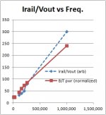
I measured the current draw from the power supply as a function of frequency. Classic increase in current showing evidence of cross-conduction. I never ran the simulations at such high frequencies but running it this evening, I can see it there too. Attached is the measured and simulated cross-conduction current increasing with frequency. It's a very interesting thing - it appears to be greatly exacerbated by the FET gate capacitance. Even thought it occurs only at high frequencies it is far worse than the native P3a and I want to address it with some changes. I have some ideas!
Plot: the blue dashed line is the measured supply rail current (divided by output voltage to remove the effect of the falling frequency response). the red line is simulated output device power dissipation normalized to the blue line so they can be plotted on the same chart. What you see is the cross-conduction current (& BJT power dissipation) increasing (vertical axis) with frequency (horizontal axis).
I would like to hear it with the simple VAS too, but I may be too lazy to do that soon. I believe the enhanced VAS has too many benefits to ignore. There's two things going on here a) the enhanced VAS and b) two pole compensation. I've combined them but they could be applied separately. You could apply the two-pole comp to the single VAS.
Actually, it's not really an enhanced VAS - that's a poor description. It's really an enhanced Singleton input. You see, the real purpose of Q3 is to provide a bootstrap for the collector load of Q1. This increases the effective collector load impedance. It reduces the current fluctuations through Q1 rather like a CFP input would but instead of being a local feedback loop like a CFP it makes the extra gain available to the whole amplifier - or R8 can be used to keep it to the VAS stage. I first applied this idea in TGM6, using a CFP topology. TGM8 uses a topology more similar to TGM7 which is also got a bootstrapped input stage. However, in TGM8 this bootstrap requires no capacitor and is extremely fast. It's a superb input stage as far as I am concerned and this is the first time I've ever seen it used - I think it will get used by others when they recognize what it brings to the table. So I'm inclined to keep it 😀
I have modeled the current sharing. The BJT should provide all the output current up to around 2.4A at which point the FETs turn on. The FETs don't protect the BJTs forever, at some higher current the BJTs will provide more current - especially into a low load impedance. The amp will still blow up if you short the output.
The heating that was bothering me before - I realized what it is. And it isn't good. I believe it's cross conduction. This is where the outputs don't turn off fast enough and so the overlap region where both the NPN and PNP devices are conducting is larger. It is worse with CFP output stages than double EF because you can't install a 'speed up capacitor' to suck the minority charge carriers out of the bases of the power devices.
I measured the current draw from the power supply as a function of frequency. Classic increase in current showing evidence of cross-conduction. I never ran the simulations at such high frequencies but running it this evening, I can see it there too. Attached is the measured and simulated cross-conduction current increasing with frequency. It's a very interesting thing - it appears to be greatly exacerbated by the FET gate capacitance. Even thought it occurs only at high frequencies it is far worse than the native P3a and I want to address it with some changes. I have some ideas!
Plot: the blue dashed line is the measured supply rail current (divided by output voltage to remove the effect of the falling frequency response). the red line is simulated output device power dissipation normalized to the blue line so they can be plotted on the same chart. What you see is the cross-conduction current (& BJT power dissipation) increasing (vertical axis) with frequency (horizontal axis).
Attachments
Last edited:
I'm glad you explained that the two-pole compensation and enhanced Singleton input are actually two separate elements, because I couldn't find any description of a transistor (Q3) in any of the literature I've been reading that deals with compensation schemes! I've been wondering about this part of the circuit for a while, which is part for my reluctance to build it.
If I wanted to try two-pole compensation with the simple input stage, am I correct in thinking that:
R4 = 0R
Q3 = unpopulated
C4 = 22p
C6 = 330p
R7 = unpopulated
A wire link between Q3 collector and emitter pins
Conversely, if I wanted to try the bootstrapped input stage with dominant pole compensation:
R4 = 1k
Q3 = populated
C4 = 68p
C6 = wire link
R7 = populated
It is possible to use nested feedback with either dominant pole or 2-pole compensation schemes.
Output transistors
Since you have only (so far) tested the BJT+FET combo, I thought you might be interested to know that I've experienced none of the output transistor overheating issues on my boards with only the BJTs populated.
I don't have a signal generator to inject high frequency signal but testing with music signals at high output levels (into speakers and a dummy 8R load) the output temps are line ball with a P3A.
- Home
- Amplifiers
- Solid State
- TGM8 - my best amplifier, incredible bass, clear highs, no fatigue (inspired by Rod Elliot P3a)