I was hoping that with cascoded outputs that the increased capacitances of the drive MOSFETs would a relatively minor issue. Perhaps I have a serious gap in my knowledge about cascoded stages. I haven't seen discussions of the capacitance effects due to the cascode devices or parameters of them that should be optimized.And there you have it. Probably the next issue you might want to think about
is the increased capacitance of the gain devices operated at 3 volts.
😎
Other than increasing Vds of the drive MOSFETs or using a lower impedance driver circuit, what can be done to reduce the effects due to these capacitances?
lhquam. Thank you for the data. What is the average Gate-Source voltage; not shown in the latest schematic.The F5 does not have the output offset problem because it is entirely DC coupled, thus the negative feedback applies to output offset as well as to AC voltage.
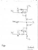
Here is the schematic with some voltages added.
With all due respect, the proposed circuit [feedforward] is DC coupled like diyF5. I will use your data to generate a "functional" schematic to analyze its feasibility.
Best regards
Antoinel said:I expected a 6L6 tube for scale 🙂
Lol... You are right, I should have done that!!
😀 😀 😀
Last edited:
Your diyF6 build is great, and professional.Lol... You are right, I should have done that!!
😀 😀 😀
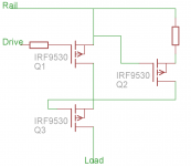
Woudl this work?
Q2 is having nuttin' to open it (remember enhanced vs. depletion ) ...... and - even if it have summetin' , it's current will have nowhere to go

Antoinel said:Your diyF6 build is great, and professional.
Thanks! Can you tell me how it looks? I am also still not sure how much space I should have in-between the chassis halves - What did I decide on? You must be Antoinel from the future... I haven't done the F6 yet... 🙂 🙂 🙂 🙂 🙂
All kidding aside, thanks for the comments, you are probably meaning to have typed F5 or F4.
The F6 is on the docket and a little different than the others - I am going to have the PSU and the amp in 2 chassis. (For modularity, and more amps in the future, cheaper.)
I am going to have the PSU and the amp in 2 chassis. (For modularity, and more amps in the future, cheaper.)
Exactly my thoughts about my F6 🙂
Plus it should be safer with the trafos...

Maybe best of all worlds. A proposed buffer circuit is attached. Complementary enhancement JFETs or bjts; your choice.I was hoping that with cascoded outputs that the increased capacitances of the drive MOSFETs would a relatively minor issue. Perhaps I have a serious gap in my knowledge about cascoded stages. I haven't seen discussions of the capacitance effects due to the cascode devices or parameters of them that should be optimized.
Other than increasing Vds of the drive MOSFETs or using a lower impedance driver circuit, what can be done to reduce the effects due to these capacitances?
Attachments
and then there goes simplicity outa window.........
even if idea is interesting , per se .......
remember that all 3 (4) windings in F6 are the same , so you're having same AC on disposal ( to feed output gates ) , having it through or without xformer , when input buffer is used
even if idea is interesting , per se .......
remember that all 3 (4) windings in F6 are the same , so you're having same AC on disposal ( to feed output gates ) , having it through or without xformer , when input buffer is used
Last edited:
and then there goes simplicity outa window.........
even if idea is interesting , per se .......
remember that all 3 (4) windings in F6 are the same , so you're having same AC on disposal ( to feed output gates ) , having it through or without xformer , when input buffer is used
Thanks Zen Mod. Please show a clarifying schematic as your time allows. One may also consider a quasi P-channel complement of R100A [or other JFET] by compounding it with a leading small signal bjt; for example. Mr. Pass used quasi PNPs in older work you showed in a post of Papa's Pub's. It is less symmetric; but the input capacitance presented to the secondary windings is like that in diyF6.
Last edited:
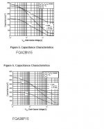
I went with the FQA28N15 and FQA36P15 primarily for their high transconductance. Given that Vdsmax and power dissipation requirements are lower for the drive FETs, I could probably find a N/P FET pair with better characteristics. How about sending me some LU1014s and their P-channel complement? 😀And there you have it. Probably the next issue you might want to think about
is the increased capacitance of the gain devices operated at 3 volts.
😎
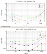
Next task: run the sweeps without the cascode FETs, and with the cascode FETs at a higher voltage.
Here is a comparison of my F6CC with and without cascoding. The left plots are with cascoding and Vds=3V on the drive FETs. The right plots are without cascoding. In both cases adjustments of P3 and P4 were made to minimize H2 as 1kHz, 1watt.
What is really interesting is the difference at 10 watts, and how flat the THD curve is for the cascoded circuit.
What is really interesting is the difference at 10 watts, and how flat the THD curve is for the cascoded circuit.
Attachments

Last edited:
These are nice comparisons - thank you for posting them.
If you do try the cascoded circ at some point, there are a lot of new and many not-so-new N channel low (and flat) Ciss Fets that you can use in the outputs. You might find that you like the results quite a lot - even without cascoding.
If you do try the cascoded circ at some point, there are a lot of new and many not-so-new N channel low (and flat) Ciss Fets that you can use in the outputs. You might find that you like the results quite a lot - even without cascoding.
Are there any N/P complements with those characteristics?These are nice comparisons - thank you for posting them.
If you do try the cascoded circ at some point, there are a lot of new and many not-so-new N channel low (and flat) Ciss Fets that you can use in the outputs. You might find that you like the results quite a lot - even without cascoding.
Wow, I guess I've been kind of snoozing, and preoccupied with life changes, and haven't been on Pass Labs forum for awhile and just saw this thread. 😕 Great thread and lots of cool ideas and circuits shared here. Very nice amp and article Nelson! Thanks for sharing again ... and to everyone else too.
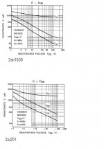
I think you know the 1530/201 pairs and they may be worth a try. I used the n channel only and found it pretty decent. These might do better in your design compared to some direct coupled designs due to their low Vth. The p channel 201s, I haven't tried apart from just measuring them but many say that they are good.
Last edited:
- Home
- Amplifiers
- Pass Labs
- F6 Amplifier