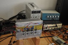
Will the heat sink be cooled by forced-air?I received my F6CC Teaser boards and parts. Here is a picture of the build so far. Obviously the MOSFETs have not been yet attached with mica and grease. I am about ready for a smoke test.
This is a bench-test setup where the MOSFETs are attached using MOLEX connectors and elevated by a 1/4" aluminum plate which is attached to the heatsink with thermal grease and screws. This makes it easy to experiment with different MOSFETs be unscrewing them and readjusting the bias voltages. Also, using hex standoffs for power and output connections makes board removal easy in order to make component changes.
Assuming roughly F5 power dissipation, ie. 65 watts/channel, the heatsink should be adequate for convection cooling. It is from HeatsinkUSA: 10.8" wide, 7" long, and 2.5" fin height. 10.080" Wide Extruded Aluminum Heatsink - HeatsinkUSA, LLC StoreWill the heat sink be cooled by forced-air?
Have you considered a simple regulated cascode as a way of avoiding Rs? Would this allow a type of active degeneration of the cacode device, and with it, the fet it guards.
As I have repeatedly stated, with the transformer secondaries connected to the MOSFET source pins, there is no AC degeneration, and the source resistor only affects DC bias stabilization. Same in the F6.Have you considered a simple regulated cascode as a way of avoiding Rs? Would this allow a type of active degeneration of the cacode device, and with it, the fet it guards.
What you are suggesting could be accomplished in a simpler manner using a DC current servo in the gate bias circuit. Here is an example of a design for a cascoded F5 with no AC degeneration using a current servo:
Attachments
way of avoiding Rs?
The F6 can be built without Rs affecting either AC degenration or DC bias. It would appear, that this is how Nelson chose to do it in his sample sent to 6moons. Clever control of the cascode could possibly accomplish this. I am new to the lingo, but i assume that a servo is the same as an error amplifier.
Thanks lhquam for the valuable info.Assuming roughly F5 power dissipation, ie. 65 watts/channel, the heatsink should be adequate for convection cooling. It is from HeatsinkUSA: 10.8" wide, 7" long, and 2.5" fin height. 10.080" Wide Extruded Aluminum Heatsink - HeatsinkUSA, LLC Store
DC servo is a fascinating development; maybe a first to use an op amp in this thread or even the Pass Labs Forum.As I have repeatedly stated, with the transformer secondaries connected to the MOSFET source pins, there is no AC degeneration, and the source resistor only affects DC bias stabilization. Same in the F6.
What you are suggesting could be accomplished in a simpler manner using a DC current servo in the gate bias circuit. Here is an example of a design for a cascoded F5 with no AC degeneration using a current servo:
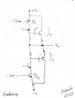
A possible idea to stabilize the bias of the output stage will be to idle Q1 and Q2 at a lower current, and simultanously augment the needed total output current with [n] complementary current bootstraps; shown as bjts for example. This proposed circuit [attached] develops a constant voltage across Q1 and Q2 [your cascodes], and a simultaneous contant current flowing through them. This thinking was borrowed from US 4,107,619 which is STASIS[R] for the amps of Threshold Corp.
It is possible that this circuit may also function as a souped up F5!
It is possible that this circuit may also function as a souped up F5!
Attachments
No smoke! 🙂 The board layout appears to be fine, except that the pots are backwards wrt. clockwise increasing the relevant parameter (no big deal).
The overall bias current stability is fine, except that the output offset voltage drifts more than I would like. Is this problem related to the cascoded outputs? If so, there might be a simple 2-resistor solution based on negative feedback to the bias circuits.
The THD measurements are OK, but not as good as I am looking for. There is still a lot of tweaking to do.
Attachments
Very excellent. The temperature drift probably relates most to the
low voltage across the cascoded Mosfets, and the failure to be able to
match the coefficients of N and P devices.
What Vds are you running on the devices?
😎
low voltage across the cascoded Mosfets, and the failure to be able to
match the coefficients of N and P devices.
What Vds are you running on the devices?
😎
Very excellent. The temperature drift probably relates most to the
low voltage across the cascoded Mosfets, and the failure to be able to
match the coefficients of N and P devices.
What Vds are you running on the devices?
😎
Currently Vds is about 3 volts, but easy to adjust with pots.
I believe that the DC offset problem is due to lack of any DC negative feedback. In the F6, the upper bias circuit couples to the output voltage, providing negative feedback to stabilize the offset voltage. In my F6CC, both bias circuits are referenced to the rails. By removing the cascode FETS and jumpering source-to-drain, I can easily verify whether the stability issue is due to cascoding.
Last edited:
it's begging for rails voltage decrease ; even if cascoded , I believe entire shebang will behave sweeter having more proper voltage across cascoded (active) mosfets
that's at least my experience with Jfets - in yore , when I compared Papa Borbely approach ( "voltage starved" ) vs. Papa approach (put them in sweet spot and cascode)
that's at least my experience with Jfets - in yore , when I compared Papa Borbely approach ( "voltage starved" ) vs. Papa approach (put them in sweet spot and cascode)
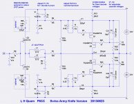
I found a 2 resistor "solution" to the output offset issue as shown below. R15 and R16 provide negative feedback to the bias voltages sufficient to stabilize the output offset voltage. Because of the symmetric nature of the feedback, the output offset is largely insensitive to equal changes in the rail voltages due to an AC mains voltage change. The downside is that the idle current changes 28ma per volt change on 120V mains. Thus if the amplifier is biased for 1.3A at 120 volts, the bias will drop to 1.244A at 118V on the mains. I have not found a simple circuit that does any better.
Attachments
Will the [feedforward] proposed approach in post# 4381 help? Does diyF5 have the difficulty Teaser F6CC have?
Please show on your schematic the voltage drop across R25, R26 [on drains of front end], and Vgs for Q1 and Q2.
Thanks and best regards
Please show on your schematic the voltage drop across R25, R26 [on drains of front end], and Vgs for Q1 and Q2.
Thanks and best regards
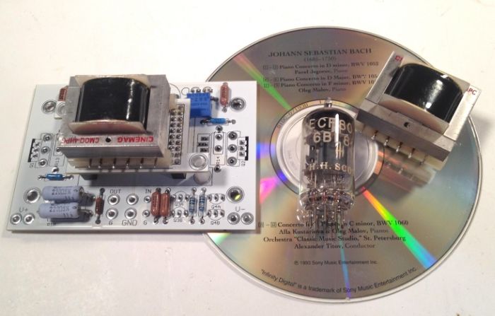
I received my CineMag transformers yesterday, they are much smaller than I was envisioning - rather jewel-like and precious. There is no doubt that they are of the highest quality.
Now that I can determine the height of the PCB assembly, from the face of the output transistors to the top of the signal transformers I can finalize the layout of the chassis. (It's going to be as narrow as I can comfortably make it.)
Here is a photo for scale -
Now that I can determine the height of the PCB assembly, from the face of the output transistors to the top of the signal transformers I can finalize the layout of the chassis. (It's going to be as narrow as I can comfortably make it.)
Here is a photo for scale -
An externally hosted image should be here but it was not working when we last tested it.
I received my CineMag transformers yesterday, they are much smaller than I was envisioning - rather jewel-like and precious. There is no doubt that they are of the highest quality.
Now that I can determine the height of the PCB assembly, from the face of the output transistors to the top of the signal transformers I can finalize the layout of the chassis. (It's going to be as narrow as I can comfortably make it.)
Here is a photo for scale -
I expected a 6L6 tube for scale.🙂
I found a 2 resistor "solution" to the output offset issue.
And there you have it. Probably the next issue you might want to think about
is the increased capacitance of the gain devices operated at 3 volts.
😎
as said in #4673 ......... but , as usual , nobody is noticing what I'm writing ......... most probably because I already had fair share of writing nonsense


Will the [feedforward] proposed approach in post# 4381 help? Does diyF5 have the difficulty Teaser F6CC have?
Please show on your schematic the voltage drop across R25, R26 [on drains of front end], and Vgs for Q1 and Q2.
Thanks and best regards
The F5 does not have the output offset problem because it is entirely DC coupled, thus the negative feedback applies to output offset as well as to AC voltage.
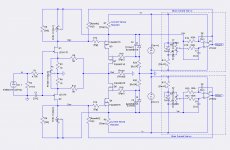
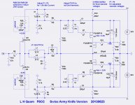
Here is the schematic with some voltages added.
Attachments
- Home
- Amplifiers
- Pass Labs
- F6 Amplifier