If I was to go the switchmode route, I'd design my own magnetics. It's not that hard, though, sourcing bobbins, cores, etc. can be a bit tricky. However, switchmode design is not trivial -- especially not when higher voltages are involved. Been there, done that, fried those parts. The main issue with tube supplies is that they tend to be hundreds of volts at hundreds of mA. So... hundreds of watts. The one for my 300B amp will need to supply 475 V @ 90 mA plus -150 V @ 10 mA per channel. So just north of 100 W for a stereo amp. It may be possible to find a shortcut by using the Nixie with a higher input voltage, but to me it loses some of its attractiveness when you connect a complex switcher to a bulky mains transformer.
600+ V caps... Yeah. Usually not store parts. 400 V are common. As are 450 V, though to a lesser extent. I use two 400 V caps in series for my supply.
~Tom
600+ V caps... Yeah. Usually not store parts. 400 V are common. As are 450 V, though to a lesser extent. I use two 400 V caps in series for my supply.
~Tom
I'd agree switchmode is more admissable for signal tubes than power tubes---doesn't take all that much investment in the magnetics for boosting a lower supply before the cost becomes comparable to a higher power trafo and the regulator of post 129. It's an interesting option to consider though.
I'd agree switchmode is more admissable for signal tubes than power tubes---doesn't take all that much investment in the magnetics for boosting a lower supply before the cost becomes comparable to a higher power trafo and the regulator of post 129. It's an interesting option to consider though.
Otherway round... I use Boost mode PFC for power tube B+ with excellent regulation. All this switchmode is no mean thing, it requires a learning curve and with it the EMC principles with considerable complexity. There are nice functions like ramp up and chosing a voltage that suits the circuit. Those like myself who did RF & magnetics engineering as a career during the 1960's and onwards have a knowledge Vorsprung over todays lot, especially when everything was worked out by sliderules (still use it).
I am still baffled how alot of so called transformers experts of today simply don't "get it"....caused by the lack of experience.
I agree about costs and the physical problems of actually fitting it in a chassis. Requires planning.
richy
Attachments
Otherway round... I use Boost mode PFC for power tube B+ with excellent regulation. All this switchmode is no mean thing, it requires a learning curve and with it the EMC principles with considerable complexity.
Very true. I've dabbled some in switchmode supply design. I designed a 500 W converter for use in an audio amp back in the late 1990'ies. +/-60 V, +/-45 V out; 220 VAC in. No PFC, though. So I'm not afraid of it. But I respect it and know that it comes with some non-insignificant challenges. It's a project with a scale of complexity that's probably bigger that that of the amp it's supplying. Although, my linear regulator adventure is turning into that as well.... 🙂 Sourcing the magnetic components can be a royal pain these days as well. Unless..... Do you have a good source for magnetics (bobbins, cores, etc)? Specifically, the RM cores are nice.
~Tom
Alot of the sources I had/knew from the early 1980/90's have dried up changed name and awkward to track down; the excellent amorphous materials by the Allied Signal, so effective for CM chokes etc often came to the rescue in a "tight design". Company changed to AMOS I believe. Since the biscuit tin approach is inevitable for EMC compliance & screening at high powers, Farnell (Newark in US) has feedthough ceramic caps and my stach of traditional cores, ETD,E's etc for continuous gradually heads towards Planar, although this design isn't good for discontinuous operation.
My best designs are with the TDK PQ style, my previous stocks created from a decade a as freelance R&D engineer in large MiL corporations when sales departments from Magnetic vendors gave the stuff away.. Farnell holds alot, Distrelec/European is expensive. The days aren't what they used to be.
SMPS in tube amps hasn't taken off.....the advantages of slow ramp up and such as wide flexibility of voltages and operating points.
An example..There comes a point of what to do with a 150W power amp with 600V B+, biassed for such poke and just used for 5W easy listening ? Many operators opt for increasing the grid bias volts leaning towards class B/C operation to cut down on dissipation, but I find in each and every case the top end quality deteoriates. The best solution is to switch the B+ down to 200V and ramp down grid bias into suit and this preserves the audio quality. To do this requires a logic delay ramp/up/down but integrated with a PFC offers excellent flexibility.
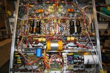
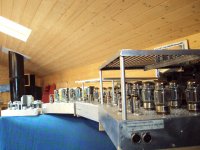
pic enclosed....These gentle giants have switchable power settings that greatly saving unwanted dissipation without rubbing quality.
I would have thought that ferrite stuff is easy to get hold off in the US. George/TubeLab might know.
richy.
My best designs are with the TDK PQ style, my previous stocks created from a decade a as freelance R&D engineer in large MiL corporations when sales departments from Magnetic vendors gave the stuff away.. Farnell holds alot, Distrelec/European is expensive. The days aren't what they used to be.
SMPS in tube amps hasn't taken off.....the advantages of slow ramp up and such as wide flexibility of voltages and operating points.
An example..There comes a point of what to do with a 150W power amp with 600V B+, biassed for such poke and just used for 5W easy listening ? Many operators opt for increasing the grid bias volts leaning towards class B/C operation to cut down on dissipation, but I find in each and every case the top end quality deteoriates. The best solution is to switch the B+ down to 200V and ramp down grid bias into suit and this preserves the audio quality. To do this requires a logic delay ramp/up/down but integrated with a PFC offers excellent flexibility.
pic enclosed....These gentle giants have switchable power settings that greatly saving unwanted dissipation without rubbing quality.
I would have thought that ferrite stuff is easy to get hold off in the US. George/TubeLab might know.
richy.
Attachments
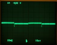
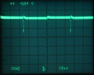
Transient response
This regulator is really quite well-behaved. The measurements were done at 20 kHz with a 25 % load step. The regulator barely flinches when the load is shed. It gives a 0.5 us blip when the load is increased. The zoom view shows the blip at load increase.
I do see about 1.3 mVrms of 60 Hz on the output, which is the cause of the fat-looking trace. I believe that was caused by a layout snafu. It turns out I ran the most sensitive node in the circuit for quite a ways. That's an excellent injection point for inductive coupling as any current injected on that node sees about 120 dB of gain to the output. Shielding with some copper tape reduced the 60 Hz component by about 10 %. Thankfully, it's pretty easy to reduce the area of that loop.
~Tom
Attachments

Last edited:
Shooting spikes in single layer boards is the cause of so many SS problems and often ruins the CM rejection. If in doubt go to the double side ground plane technique which requires more work but is near perfect. By putting foil on after and soldered in various places is in effect doing the same.It is a fact that most PCB designers leave the supply routing last with invariably poor decoupling.
If in doubt go to the double side ground plane technique which requires more work but is near perfect. By putting foil on after and soldered in various places is in effect doing the same.It is a fact that most PCB designers leave the supply routing last with invariably poor decoupling.
One has to be careful with just blindly pouring ground planes, though. They couple to everything and unless you employ moating or other fancy techniques, you have no control over the return currents.
In addition to reducing the routing length and loop area, I'll probably make a small pour around the sensitive node and ground it appropriately.
~Tom
I find it rather impressive to watch the output voltage of this regulator on my 6-digit DMM. The output voltage is rock solid at 474.864 V +/- 1 mV even when loaded by my 300B amp. The biggest contributor to long-term drift is the temperature coefficient of R8. Blowing air across it causes the output voltage to drop some 50-ish mV... 🙂
~Tom
~Tom
Do you have your test circuits for supply measurements documented? I would *love* to see those.
~Tom
I do the same tests that Walt and Jan did for their 1995 TAA articles, line rejection (crosstalk), noise and output impedance. While the instrumentation is a bit better 16 years on, I am always in awe of the Z(out) measurements done with the diligence of Walt Jung.
I will get around to HV regulators, but they obviously require a lot more protection of the instrumentation.
One has to be careful with just blindly pouring ground planes, though. They couple to everything and unless you employ moating or other fancy techniques, you have no control over the return currents.
In addition to reducing the routing length and loop area, I'll probably make a small pour around the sensitive node and ground it appropriately.
Ultiboard has "Keep-in/Keep-out" layer, which, I guess, is "moating". Island removal is a bit of a PIA with UB.
Walt Jung discusses the layout of the Super-Regulator boards on his site, archived here: http://waltjung.org/PDFs/Regs_for_High_Perf_Audio_3.pdf He and Jan ran the high current traces on the outside of the PCB. Z(out) is improved if you can "sense" the voltage at the load via a separate connection to the error amplifier.
I do the same tests that Walt and Jan did for their 1995 TAA articles, line rejection (crosstalk), noise and output impedance.
That would be the measurement setups outlined in the first article of the series, I assume. http://waltjung.org/PDFs/Regs_for_High_Perf_Audio_1.pdf
I will get around to HV regulators, but they obviously require a lot more protection of the instrumentation.
Yep. Also, the 4700 uF cap used for the Zout measurement in Jung's article is going to be mighty hard to source for 500 V... 🙂 I'm thinking to build an electronic load. Basically, a current sink with a relatively high bandwidth modulation input. An op-amp and a MOSFET should do the job.
Ultiboard has "Keep-in/Keep-out" layer, which, I guess, is "moating". Island removal is a bit of a PIA with UB.
A moat is what separates a ground plane island from the rest of the plane. I.e. the white geometry in Fig 10 of this ADI Ground Bounce article. In Orcad, it's called anti-copper. I suppose you can use keep-in/keep-out but anti-copper is easier if you have the option.
He and Jan ran the high current traces on the outside of the PCB. Z(out) is improved if you can "sense" the voltage at the load via a separate connection to the error amplifier.
Kelvin connections are your friend for high current applications. That's for sure.
~Tom
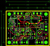
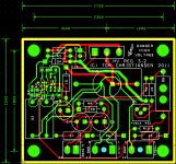
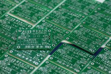
New layout
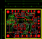
Turns out a couple of layout optimizations could be done. As reported yesterday, I found that the most sensitive node in the circuit had been routed quite a ways. I have reduced that routing from about 1020 mil (26 mm) to about 350 mil (9 mm). This was accomplished by rotating U1, U2 and associated components and by changing R1, R2, C2 to 0805 size SMD. In addition, D1 moved to the other side of C1, which shortened the supply routing for the floating part of the regulator considerably. Aside from the footprint changes mentioned, there were no changes to the schematic.
Then the routing was further optimized, the overall philosophy being to minimize loop areas on sensitive nodes and keeping high-current forward and return paths parallel/differential.
~Tom
Attachments
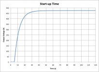
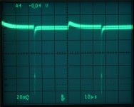
Measurements: Start-up Time
The regulator provides a nice smooth start-up. Almost like a tube rectifier. I hear no thumps in the speaker when my amp is powered up. Not even if I power up the B+ with the filaments preheated. See attached. The power was turned on at the mains switch at t = 5 seconds.
~Tom
The regulator provides a nice smooth start-up. Almost like a tube rectifier. I hear no thumps in the speaker when my amp is powered up. Not even if I power up the B+ with the filaments preheated. See attached. The power was turned on at the mains switch at t = 5 seconds.
~Tom
Attachments
Ray - it's certainly getting there... So far, I've only measured with one output device connected. I should verify with both of them. I don't see that changing things significantly, but I should check.
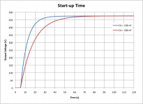
Decided to mess with the capacitors a bit. Specifically, C4 (the one from the reference to GND). It affects the residual ripple/hum on the output quite a bit. With C4 = 100 nF, I get about 1.4 mVrms of hum. Increasing C4 to 200 nF, drops the hum to 670 uVrms, but also lengthens the start-up time. No surprises here. In the final PCB, I think I'll just leave enough room so that I can stuff a 220 nF cap in for C4 and call it good. Then people can stuff it with 100 nF by default, or 220 nF if they want to accept the longer start-up time in exchange for lower residual hum.
With the amp connected, I don't hear or measure any 60 Hz hum at the speaker even with C4 = 100 nF, so the residual hum is obviously not an issue for me.
~Tom
Attachments
Last edited:
Ready for prime time
Good news: The regulator is stable at loads anywhere from 0 mA to 300 mA with and without capacitive load. The output impedance at audio frequencies is very low (<0.1 ohm @ 20 kHz).
So I made a couple of discoveries:
1) The regulator had a slight tendency to oscillate at 6 MHz with an amplitude of about 20 mVpp. At heavier load (200 mA and above), the oscillations would prevent the circuit from regulating and parts started poofing.
2) I had originally put two output devices on the regulator as I was concerned about start-up into a capacitive load. However, with the slow start-up of the regulator, two output devices are no longer needed. It's a 230 W device, so as long as its temperature is kept under control (read: mount it on a large heat sink), everything is fine.
The oscillations were due to lack of phase margin. The input cap on the MOSFET forms a pole in the MHz range with the output impedance of the op-amp. This reduces the PM and the circuit starts oscillating. To make matters worse, the input capacitance of the op-amp is actually rather high -- about 25 pF. Slowing the feedback down a bit by inserting a 10 kOhm resistor from Vout to IN(-) on the op-amp solved this.
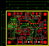
I cleaned up the layout and am about ready to push the [SUBMIT] button and have it fab'ed professionally.
Below is a few of the results as well as the new layout. The transient response on the left shows Vout (AC coupled) with 250 mA constant current, 15 mA step. On the right, it's 50 mA constant current, 15 mA step. As the step on the right is a bigger percentage of the constant output current, the glitches on the load step are bigger. No surprises here. Note that we're talking 80~100 mV of glitch on a 475 V supply.
~Tom
Good news: The regulator is stable at loads anywhere from 0 mA to 300 mA with and without capacitive load. The output impedance at audio frequencies is very low (<0.1 ohm @ 20 kHz).
So I made a couple of discoveries:
1) The regulator had a slight tendency to oscillate at 6 MHz with an amplitude of about 20 mVpp. At heavier load (200 mA and above), the oscillations would prevent the circuit from regulating and parts started poofing.
2) I had originally put two output devices on the regulator as I was concerned about start-up into a capacitive load. However, with the slow start-up of the regulator, two output devices are no longer needed. It's a 230 W device, so as long as its temperature is kept under control (read: mount it on a large heat sink), everything is fine.
The oscillations were due to lack of phase margin. The input cap on the MOSFET forms a pole in the MHz range with the output impedance of the op-amp. This reduces the PM and the circuit starts oscillating. To make matters worse, the input capacitance of the op-amp is actually rather high -- about 25 pF. Slowing the feedback down a bit by inserting a 10 kOhm resistor from Vout to IN(-) on the op-amp solved this.
I cleaned up the layout and am about ready to push the [SUBMIT] button and have it fab'ed professionally.
Below is a few of the results as well as the new layout. The transient response on the left shows Vout (AC coupled) with 250 mA constant current, 15 mA step. On the right, it's 50 mA constant current, 15 mA step. As the step on the right is a bigger percentage of the constant output current, the glitches on the load step are bigger. No surprises here. Note that we're talking 80~100 mV of glitch on a 475 V supply.
~Tom
Attachments
Last edited:
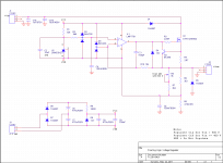
Final schematics and bill-of-materials
The final schematics and bill-of-materials attached. Enjoy. I have included the Digikey part numbers, but, of course, the parts can be obtained elsewhere as well.
~Tom
The final schematics and bill-of-materials attached. Enjoy. I have included the Digikey part numbers, but, of course, the parts can be obtained elsewhere as well.
~Tom
Attachments
Last edited:
Just out of interest (although somewhat related to the thread title) has anyone tried making an HV shunt regulator out of a string of 6.2V zeners?
I.e. for 200V just strung 32 zeners on a veroboard?
I.e. for 200V just strung 32 zeners on a veroboard?
- Status
- Not open for further replies.
- Home
- Amplifiers
- Power Supplies
- High Voltage Regulators (Maida or zener)