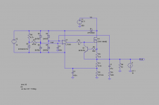
Coupling the plus input to ground via a 100Hz lowpass seems likely to cause problems as shifts in the op amp supply will cause the percieved reference and hence Vout to change. I'd tie C3 to the negative op amp rail, which has the side benefit of making D3 and D4 unnecessary (as an aside, the schematic above connects them on the wrong side of R7). Values of C3 around 10u are interesting as Q1 and R3 could potentially be removed.
A cap in parallel with R2 requires caution as its high value means not much cap is needed for the resulting lowpass filter to corner within audio bandwidth.
Agree the local loop's probably not needed with a 7707 but good to have available.
A cap in parallel with R2 requires caution as its high value means not much cap is needed for the resulting lowpass filter to corner within audio bandwidth.
Agree the local loop's probably not needed with a 7707 but good to have available.
In a more recent sim, I coupled both the reference and the negative supply rail of the op-amp to ground without issues (at least as far as ripple rejection and short circuit survivability goes). 100 nF were used. I also spotted R7 on the wrong side of the diodes and moved it as you suggested.
I see your point with the cap across R2. Don't know if it's an issue or not. It may screw up the output impedance. More sims needed.
Semantics: The LMP7707 is actually uncompensated and will need a compensation cap. I am planning to use the internally compensated version, LMP7701. I didn't even realize that people still made uncompensated op-amps in this day and age...
~Tom
A grounded reference creates a feedback loop with gain R2/R1. So differences in the ground potentials of R2 and C3 at frequencies above the R7-C3 cutoff will get amplified by up to 45dB. Given good layout this won't matter much but IMO it's better to avoid the issue---while I'm not seeing the feedback would cause instability I'd bet things would run quieter with C3 going to the op amp's negative rail.
The example which immediately springs to mind is Vin dropping below the point where Vout can be maintained---the most common case being a main sags below -15% or so (EPRI data says this happens all the time). Suppose mains droop causes Vout to go to 475V instead of the target of 480V. R7 means the voltage across C3 will stay near 480V, taking the reference to 7.5V and making the regulator want a 1.5kV output. The resulting loss of regulation for the R7-C3 time constant's not a big deal if everything hanging off Vout can handle the maximum Vin. For example, the mains could potentially rebound enough after the droop to take Vin to 700V (though most of the probability distribution's below 625V). If you're counting on the regulator to protect 500 or 600V parts hanging off Vout this is a problem.
The example which immediately springs to mind is Vin dropping below the point where Vout can be maintained---the most common case being a main sags below -15% or so (EPRI data says this happens all the time). Suppose mains droop causes Vout to go to 475V instead of the target of 480V. R7 means the voltage across C3 will stay near 480V, taking the reference to 7.5V and making the regulator want a 1.5kV output. The resulting loss of regulation for the R7-C3 time constant's not a big deal if everything hanging off Vout can handle the maximum Vin. For example, the mains could potentially rebound enough after the droop to take Vin to 700V (though most of the probability distribution's below 625V). If you're counting on the regulator to protect 500 or 600V parts hanging off Vout this is a problem.
Last edited:
Assuming the negative feedback loop through R4, M1, R3 is dominant, the op-amp will maintain Vref across R1. This sets up a current in R1, thus, R2, which establishes the output voltage. So far so good...
Now, mind you that in the schematic, R7 is on the wrong side of the diodes. In reality, it'll be connected between Vref (V3) and the diode clamp. In the event that the output voltage drops dramatically (overload), the negative rail for the op-amp will drop also. The positive op-amp rail tracks the negative rail and C3 is discharged through D3 (again, recall that R7 is between V3 and D3, D4).
Now in the case of a sagging input voltage (yes, it does happen all the time): Vin drops, hence Vout drops. Let's say Vin drops to 475 V and the nominal output voltage is supposed to be 480 V. As Vin goes below 480 V, Vout will start to drop (this probably will happen before Vin = Vout, due to the non-zero Vds on M1, but that's another story). Effectively, this raises the reference voltage as C3 remains charged. The op-amp output will saturate and force M1 into strong inversion. Vout is now equal to Vin (less a negligible Iout*Rds(ON) drop). So far, so good. No over-voltage condition on the output, no fried parts.
Now, Vin recovers to the nominal 560 V. As the output voltage recovers to 480 V, the effective reference voltage is now back down to 2.5 V (assuming C3 hasn't lost any charge). The op-amp will recover from saturation and control M1 gate, close the negative feedback loop as normal. Any over-voltage spike will be the result of the op-amp saturation recovery and bandwidth and not related to C3.
If the Vin droop is prolonged to the point where C3 has been discharged by more than 2.5 V, there will be a momentary voltage drop on the output that will last until the voltage on C3 recovers.
That's my thinking. I don't see any way Vout would be able to exceed the nominal output voltage except for a short, 1-us time frame, glitch during op-amp saturation recovery. I suspect the 47 uF cap will smooth that out rather nicely...
Actually, sim says decoupling the reference to the negative supply rail of the opamp rather than ground ruins ripple rejection. Makes a certain amount of sense. The output voltage is ground referenced. Hence, the reference needs to be also. Decoupling the reference to the negative rail makes Vref referenced to Vout. Not what you want...
~Tom
DUH! It's the diode, stupid!
Face-palm. If Vin drops below the voltage on C3, D1 conducts, thus, discharging C3. When Vin recovers, C3 will be at a low voltage, and the circuit recovers according to the time constant of C3*R7. This has been confirmed by simulation as well.
And actually... Taking D1 out, makes the circuit buzz at about 20 kHz on recovery following an input voltage droop. Low amplitude oscillation, but definitely an instability.
~Tom
Interesting result; I would have expected C1 to be large enough for U1 to hold 2.5V over R1 without letting Vout oscillate in response to ripple. Could be a model issue, could just be M1 provides enough drive to move the capacitive overshoot region up from pF to uF.
Good point on the recovery behavior. I'd missed that. 😱
Good point on the recovery behavior. I'd missed that. 😱
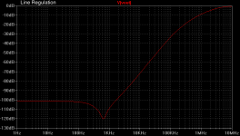
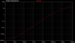
With attached regulator, sim says:
Start-up time: 30 seconds
Current limit: 290 mA
The output impedance depends heavily on the current limiter. If the current limit is raised (lowering R3), the output impedance is lowered. Same goes for the ripple rejection, actually.
With the slow start-up, the current limiter isn't technically needed. But I wouldn't mind having some protection against momentary shorts to ground.
C1, R9 represent the load of the amp I'm driving with this regulator. If this regulator was to be built as a stand-alone circuit, it would actually benefit from having as little capacitance on the output as possible. Lower capacitance allows the regulator to reduce the output impedance at higher frequencies.
~Tom
Attachments
Last edited:
Interesting result; I would have expected C1 to be large enough for U1 to hold 2.5V over R1 without letting Vout oscillate in response to ripple.
When Vin drops below Vout, C1 will discharge through the body diode of M1. I hadn't thought of that discharge path either, though, it makes perfect sense...
~Tom
Floating High-Voltage Regulator
Folks,
Attached is my latest and greatest. I have it running as a rat's nest in the lab and observe no ripple residual on the regulator output. The only oddity I see is that I have about 18 mVrms of 60 Hz on the output. I attribute this to the rat's nest layout. Had it been ripple, it would have been 120 Hz.
I should have a board thrown together for this over the weekend and will post results.
~Tom
Attachments
Hi,
I have been silently following this thread with much interest, since I was myself in the need of a similar solution about a year ago. Interestingly enough, you have reached a very similar design to the one I made, which was based on the venerable LM723 in a floating configuration.
If you look at the datasheet of this IC, you will find not only that it includes all the major components in one single package, but also that the application notes include a similar HV circuit.
My goal was initially to develop a 0..400V 150 mA lab power supply, featuring both voltage and current limiting, capable of driving it with a PIC microcontroller. For wide range variable setups, the LM723 is definitely not the best option, and now I am looking more into a discrete version inspired on the MC1466.
One advice, be extremely careful when selecting your opamp; it must be free of phase reversal, high slew rate, and preferably rail to rail. Some alternatives are the OPA2134 and LT101x.
I will try to post some schematics ASAP.
Cheers!
izozaya, it may be wise to include zener protection direct to FET gates, as per Tom's circuit - especially as you have high series resistors.
Absolutely right; also a few compensating caps to prevent unwanted oscilations and some diodes to prevent inputs to go above / below power supply rails.
Interestingly enough, you have reached a very similar design to the one I made, which was based on the venerable LM723 in a floating configuration.
If you look at the datasheet of this IC, you will find not only that it includes all the major components in one single package, but also that the application notes include a similar HV circuit.
That is true. The good ol' LM723 does have both the reference and the error amp in one package. Unfortunately, it also suffers from 1970'ies technology. The reference tempco is 150 ppm/deg C which is a bit on the high side and the ripple rejection is 70-something dB. With modern parts I expect to do better.
My goal was initially to develop a 0..400V 150 mA lab power supply
I suggest looking at the schematics for the HP 6209B 0~320 V, 0~100 mA lab power supply. You can download it as part of the service manual directly from Agilent (used to be HP). Especially the rectifier circuit is neat. It rectifies only a small, programmable part of the AC waveform, hence the input voltage to the regulator tracks the output voltage, thus, the power dissipated in the regulator is limited. Very neat.
One advice, be extremely careful when selecting your opamp; it must be free of phase reversal, high slew rate, and preferably rail to rail. Some alternatives are the OPA2134 and LT101x.
Yep. Phase reversal woud be bad. Thankfully, modern op-amps have been designed to avoid this issue... Rail-to-rail on the output as well as at least ground sensing inputs are nice to have. The LMP7701 I chose is rail-to-rail on both inputs and outputs.
My first prototype used an OPA134. It's not rail-to-rail, neither on the input nor the output, so I had to raise the reference voltage and ensure that the supply voltage was high enough that it could drive the MOSFET gate high enough. I expect these issues to go away in the final circuit.
~Tom
I've been fooling with similar ideas, though in a more modern format of using a secondary side full bridge MOSFET controller to implement a regulating synchronous rectifier rather than an SCR. Since tubes are typically class A loads it'd probably make more sense to use a conventional SMPS with soft start. The Nixie's a popular low voltage tube supply but radio supplies may be more relevant here.Especially the rectifier circuit is neat. It rectifies only a small, programmable part of the AC waveform, hence the input voltage to the regulator tracks the output voltage, thus, the power dissipated in the regulator is limited.
I've been fooling with similar ideas, though in a more modern format of using a secondary side full bridge MOSFET controller to implement a regulating synchronous rectifier rather than an SCR.
That'd work too.
The Nixie's a popular low voltage tube supply
Beware that Vin/Vout = 1-D for a boost converter. Hence for a low Vin/Vout -- as is the case for that design -- duty cycle, D, approaches 1. Unfortunately, this means that the inductor has hardly any time to dump the magnetic energy into the output cap. This causes the peak inductor currents to be rather large. I'm not saying the design is broken. I'm just expressing concern with Vin = 9 V and Vout = 220 V.
radio supplies may be more relevant here.
That lab bench is way too clean. I question the circuit design purely on those grounds.... 😛
~Tom
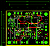
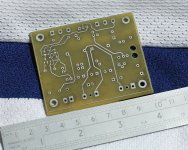
Hot off the press
I'm getting good at this here toner transfer stuff. The registration error between top and bottom layer is on the order of 0.2 mm. I'm likin' it...
Ultimately, I'm going to have professional boards made. But this'll do for the prototype.
~Tom
I'm getting good at this here toner transfer stuff. The registration error between top and bottom layer is on the order of 0.2 mm. I'm likin' it...
Ultimately, I'm going to have professional boards made. But this'll do for the prototype.
~Tom
Attachments
It's manageble on the Nixie---D is greater than 10% or so given reasonable choice of input and output voltages. A more comfortable design point would be boosting an AN-0540 or similar---operated at D = 16% it yields 100mA at 350V. Stepping up from one of Antek's tube specific trafos offers more options at reasonable duty cycles. For example, an AN-1T150 boosted to 100mA at 600V would have D = 35%.Vin/Vout = 1-D for a boost converter
Nichicon KX only goes to 450V though---not sure where one would find 600+V caps intended for use with switching supplies. The inductor might also be challenging; on a quick look I'm not seeing ones speced for withstanding voltage across the coil. Trafo leveraged boost is nicer but makes finding parts trickier (the WE-FB series is one option).
Last edited:
- Status
- Not open for further replies.
- Home
- Amplifiers
- Power Supplies
- High Voltage Regulators (Maida or zener)