A regulator should indeed be stable. And the regs I use are dead stable with 100% feedback at 20Hz and above- Tom may wish to investigate why he is unable to use more of the open loop gain available to him to reduce the ripple, noise, and bounce.
It might be useful to read the text reference I cited.
It might be useful to read the text reference I cited.
Stability and Optimised Transient Response are not the same thing.
A Stable regulator (or amplifier) is one that remains free of oscillation at all intended load levels and impedances. That simply means that the feedback signal does not rotate phase by 180 degrees by the time the gain has degraded to one in the frequency domain - for any expected operating condition.
Optimised transient response is the application of frequency compensation (poles and/or zeros) in order to yield the best-controlled output voltage waveform when the regulator faces different kinds of step loads, or other prescribed load changes. Getting this wrong for an audio amplifier's supply regulator will certainly impose unpleasant changes on the sound, since you are effectively placing a highly-distorting amplifier in series with your (hopefully) tailored-distortion valve amplifier.
Frequency compensation, applied properly, satisfies both of these.
At one extreme, we can build a regulator with 90 degrees of phase margin (i.e. perfectly Stable, never oscillates), but gives a poor reaction to step load changes - or music signals! This is especially likely when there are multiple low-frequency poles in the open loop response of an amplifier/regulator.
Increasing C1 in Tom's circuit may not affect stability, but it will seriously degrade Transient Response. Why? Because the open loop phase response of the regulator is characterised by poles formed by RC networks in the circuit - the capacitances being chiefly the FET's parasitics. The rolloff these produce must be reshaped in the closed loop to not only meet stability criteria (feedback phase less than 180 degrees at the frequency where gain drops to one, for any prescribed load) but the phase response needs to be shaped to avoid dramatic swings up & down, especially across the spectrum of the load signals (audio range in this case).
Increasing C1 may or may not violate stability criteria, but will certainly degrade transient response.
The problem can be approached by trial & error. Build a step-load (FET switched load box) and adjust the compensation network(s) until the response is as refined as can be achieved.
Hardened SPICE enthusiasts can attempt to model the open-loop phase, but data sheet values for capacitance are not reliably accurate, and change dramatically with load level. I sometimes use LTspice to find approximately where the poles are, simply to see how many compensation positions are needed. This appears to be how Tom has dealt with the problem, and it looks like good work to me. I do not believe that he can apply more open loop gain, as you suggest, without degrading phase response and/or stability - making the cure worse than the malady.
Increasing C1 in Tom's circuit may not affect stability, but it will seriously degrade Transient Response...
Increasing C1 may or may not violate stability criteria, but will certainly degrade transient response.
The problem can be approached by trial & error. Build a step-load (FET switched load box) and adjust the compensation network(s) until the response is as refined as can be achieved.
That's how I test regs as well, though using a bipolar. It's also good to verify by attaching a 10n/630V to the output of the supply, then connecting its other end to the input of an oscilloscope. Play music, loud.
The problem is that by running things on the edge, then using a cap in the feedback loop to compensate, you're optimizing for stuff that doesn't matter much (given that there's an output bypass cap) at the expense of stuff that DOES matter- ripple and noise rejection. If you can set the time constant of the RC in the feedback network (using the equivalent R, the two resistors in the chain in parallel) to a couple times higher than the ripple period, you can use the full open loop gain to cancel the audible ripple.
Naturally, you may set your own judgement criteria for your own regulator's performance, but to my mind, allowing the transient response to impose a ragged, or overshooting reaction to a step load is MUCH more injurious to an audio amp than ripple rejection. Remember, this ragged response is imposed on the load at low impedance since it is enforced by the feedback loop.
In any case, ripple can be reduced to vanishing levels simply by filtering the raw dc properly, whereas transient response cannot be bought back once you have screwed it up with incorrect frequency compensation.
In the case of a regulator that has not (or cannot) be compensated correctly, an output capacitor will usually degrade the response even further - a perfect example of that is the Maida, which has a designed load capacitance of 1uF - and degrades in performance either side of that.
I do not agree either, that Tom's circuit is running on the edge. Frequency compensation is naturally applied to any circuit of this kind.
In the case of your Maida, compensation is applied internally to the 317; the series-stacked components added to it then invalidate this compensation, which is exactly why its transient response is poor, and relies even for so-so performance, on a capacitor concealed behind a resistor. THAT is what is really 'running on the edge'.
The regs I was referring to were not Maida regs, but rather, a bipolar reg with a single error amp, same topology (different devices) as Tom's. Same with the treatment in VA3. These give excellent ripple rejection and excellent non-oscillatory response to load steps.
Without seeing the circuit, I cannot be specific, but in general terms, substituting Tom's FETs for high-voltage bipolars will involve lower series resistors (high voltage NPNs have reduced Hfe) and often, the parasitic capacitances are lower. These combine to mean that the compensation components will be quite different from a FET-based solution; values from one may not even be a good starting point for the other.
Due to second-breakdown effects on BJTs, circuits at higher voltages (much above 400V) will need more power-derating than with FETs, and margins will generally be finer in terms of heatsinks and turn-ON transients. But, within those restrictions, the transient behaviour for BJT based regs is likely to be better, since the open loop poles appear at a less intrusive frequency. Also, for the same current, the BJT has much greater gm, so the open loop output impedance is lower. For these reasons, if one is sure the pass device is tough enough for the application, the BJT may well be a better choice.
Due to second-breakdown effects on BJTs, circuits at higher voltages (much above 400V) will need more power-derating than with FETs, and margins will generally be finer in terms of heatsinks and turn-ON transients. But, within those restrictions, the transient behaviour for BJT based regs is likely to be better, since the open loop poles appear at a less intrusive frequency. Also, for the same current, the BJT has much greater gm, so the open loop output impedance is lower. For these reasons, if one is sure the pass device is tough enough for the application, the BJT may well be a better choice.
Last edited:
The argument is not "bipolars are better," the circuit can be made to work well with either device type (or even better, a mix), it's that for highest performance in the intended application, the ripple rejection needs to be improved. And I've suggested a path for doing so.
Of course, either flavour of device can be made to work reasonably well, if the supporting circuit is correctly designed. But I have shown clearly enough why your 'suggested path' of oversized capacitors in the feedback path will spoil the regulator - and Tom has already measured the degraded performance in dynamics.
Oversized? No, I wouldn't do that, and the explanation of "why" and "what is oversized" may be found in the Jones reference. "Properly sized?" Absolutely- that audible ripple can be greatly reduced if the time constant is set an octave or two below the ripple fundamental.
If you have a Large-Area FET (one with high gm) this can work really well. The best part is that compensation is not necessary.
The high gm is needed, since the dynamic output impedance is 1/gm. THe gm will vary somewhat with current, so you get a little 'distortion', but the transient response will be more civilised without the feedback loop, in many cases. The listening tests may well show an improvement - I certainly preferred regulators with low open loop gain in my power amps.
That's good input. Thanks. The STW12NK95 FET that I'm using is claimed to have gm = 12 S (@ 5 A, Vds = 15 V). Extrapolating the gm curve in the datasheet yields something like 3 S at 100 mA (my target output current). So 0.33 ohm Zout. That's non-shabby. More importantly, it remains 0.33 ohm throughout the audio range -- it should anyway.
I'm using the regulator to feed a class A amp, so there won't be much variation in the output current. Hence, I'd expect distortion caused by gm "modulation" to be fairly minimal.
~Tom
Is it in a chassis yet? Sometimes I will take a circuit, put it on a card table within a cookie tin in the middle of the room and use my SSM2019 battery powered amplifier to get away from all the 60Hz on the workbench. I also use shielded twisted pair for driving the regulators when measuring line rejection.
No chassis yet. My audio analyzer says it's 120 Hz on the output of the amp, so I wouldn't expect a chassis to make much of a difference. Better layout, quite possibly. But the shielding should mainly affect 60 Hz. With the Maida regulator, the amp was dead quiet. But the Maida didn't survive in the long run for reasons debated ad nauseum above.
Do you have your test circuits for supply measurements documented? I would *love* to see those.
~Tom
As somebody pointed out earlier, the poor regulation appears to be caused by the output impedance of the current source used to power the error amp. At least that's what Spice says and I believe it. That's also why the cascode works.
Of course I could spend some time designing a high-performance current mirror, but then why not just rework the circuit to become a diff pair with a current mirror load. That would certainly give plenty of loop gain and offer other advantages - such as the possibility to filter the reference voltage.
But a large part of me is debating whether this is supposed to be a REGULATOR project or an AMPLIFIER project. I think I would like it to be an AMPLIFIER project (that sweet 300B directly coupled contraption I keep mentioning, remember...? 🙂) So I'm thinking to jump on the zener stack with source follower. I'll post schematics and keep you updated on my progress.
~Tom
I got to thinking... A zener regulator with current limiter is likely to have relatively high output impedance due to the resistor needed for the current limiter circuit. "Relatively high" in this context would be 5~10 ohm or so. That would probably be alright, but I would prefer a lower output impedance. Although, given the DCR of the OPT does it really matter that much.... Anyway.
My latest musings go along the line of a floating regulator. Think LM317 on steroids. Basically, I'll follow the circuit in Figure 1 of National AN-178 but with a giant, high-voltage power NMOS as the pass device. The op-amp could be powered by a separate, floating winding on the mains transformer. A spare 6.3 V heater winding would work... Or some wire could be wound around the core to form a winding. That's easy...
I'm thinking to use LMP7717 for the op-amp and an LM336-2.5 for the reference voltage. The whole deal would ride on a small zener-regulated 5 V supply.
~Tom
Seems dicey; the current limiting needed to protect the pass device will create a large voltage differential across the op amp's inputs at start up. Since 40V 317s have blown in this situation I'd expect a 5.5V 7717 wouldn't last long. Similar issues exist with floating supplies since the op amp rails don't track B+.
There are Apex parts that could be used here but they're a few hundred bucks. So I'd suggest looking into implementing a discrete op amp with high voltage parts.
There are Apex parts that could be used here but they're a few hundred bucks. So I'd suggest looking into implementing a discrete op amp with high voltage parts.
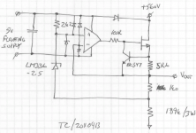
Seems I'm not communicating clearly. Attached sketches the circuit. The 5 V supply for the op-amp is floating. The range of flotation is limited to Vout~B+ by diodes. Steady-state operation should be fairly obvious. The op-amp has negative feedback, hence, will set the output to ensure that IN(+) = IN(-). This forces 2.5 V across the 1k0 resistor, which, in turn sets up the current in the feedback resistive divider.
Current limit is implemented by the 5R6 resistor and the BC547 NPN. During current limit - or short circuit - the output of the op-amp will have to track the source voltage of the NMOS pass device. Hence, the op-amp output will track Vout. This forces the negative supply rail for the op-amp to track Vout as well --> op-amp remains happy and non-fried.
It just dawned on me, though, that I'll probably have to go with a 12 V or 15 V compatible op-amp. LMP7707 would work... Vgs of the NMOS I'm using is about 4.5 V at room temp. Hence, 5 V supply is rather marginal (read not enough) -- especially at hot.
~Tom
Attachments
It does help to have a schematic. 😉 I'm not seeing this will fry but unless I'm missing something it only regulates when 560 - Vopamp_supply > Vout - 2.5, give or take a few volts if the op amp's not RRIO. The desired Vout seems be to 475V, a bit outside the common mode an OPA445 on a 90V supply floating on 560V can handle. Assuming it's desired to maintain regulation across +/-10% mains on a 520V trafo leaves me with a 2*0.1*520V + 2.5V reference + op amp rail approach limitations + ripple = 125Vish op amp supply in this topology.
I think you could get around this by floating the op amp's rails on Vout rather than Vin. Split supplies centered on Vout would probably be about right.
I think you could get around this by floating the op amp's rails on Vout rather than Vin. Split supplies centered on Vout would probably be about right.
The op-amp rails are actually floating on Vout.
Notice the polarity of the diode to Vin. It clamps the positive rail so it cannot drift higher than Vin. It is, however, free to drift below Vin. Actually, I'm not sure the diode is required. If I use a zener on the front for stabilizing the supply to the op-amp and the lower rail is clamped to Vout, the upper rail would be limited by the zener.
And actually... Now that I think about it some more. The body diode of the NMOS will clamp Vout to Vin so if the lower rail of the op-amp can't move too far anyway.
All this is really only relevant for startup, short circuit, and possibly a few failure modes anyway.
I'll see if I can get a better schematic thrown together over the weekend.
~Tom
This gets into the semantics of floating. For small op amp supply voltages the diode on the op amp's minus input clamps the minus rail to Vout + forward diode drop. The plus input is nominally at Vout---and therefore below the op amp's negative rail---so it gets clamped as well, turning the op amp into a comparator of the diodes' forward drops instead of a regulator. With the schematic above, the only reliable way I see to avoid that is to open up the op amp's supply voltage such that the diode between the op amp's positive rail and Vin forces the negative rail below Vout.
Stabilizing zeners to Vout should be much more tolerant of mains variation than a stack to Vin. E.g., 12V LMP7707, 6Vish zeners.
Stabilizing zeners to Vout should be much more tolerant of mains variation than a stack to Vin. E.g., 12V LMP7707, 6Vish zeners.

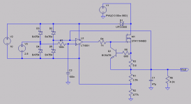
Trying LTSpice here...
C3 is needed to prevent the floating supply from bouncing once the final output voltage is reached. It also makes it real easy to implement a soft start. With the circuit as-is, it starts up in about 10 seconds.
I suspect I'll also need a cap across R2 as the negative rail for the op-amp won't be as tightly coupled to the reference node as it is in this circuit.
R6 is the load resistor.
The output voltage is 480 V. Max output current is 110 mA.
In the actual circuit, I'll add pads to form a local, high-frequency feedback loop (aka capacitor) around the op-amp. Just in case things get out of control at HF.
Sim says the ripple rejection is on the order of 100 dB(!). Boy, I hope that holds true in real life. Sounds rather optimistic, though.
~Tom
Attachments
Last edited:
- Status
- Not open for further replies.
- Home
- Amplifiers
- Power Supplies
- High Voltage Regulators (Maida or zener)