Thanks Andrew T,
To eliminate any confusion I think I'll stick to component network descriptions rather than naming rights.
Hi Powerbecker,
Thanks for those two interesting circuits. Ian Hegglun I think is an acadaemic who used to live less than 100km away in Ipswich QLD Australia at about the time of the design. Always meant to touch base.
Regarding the designs. Firstly the Marchand one is not a patch on the Simple Killer Amp. Let me explain. While it uses a similar common source output stage to achieve near R2R output stage efficiency, it does so with two prior stages of gain, the second being right on it's current modulation limit to drive the output fully - much as my Simple Killer Amp without the bootstrap C's. This undegenerated low gain stage (ignoring the level/phase shifting /current mirror) is running 50%+ modulation of current with no linearising emitter resistors so has a base/base signal handling of only 52mV (2 x 26mV intrinsic) to drive resistive collector loads at 2+Vac but DC across the Rc of only 3.5V (Vgs) so modulation and THD will be high. A further input gain stage has been necessarily added to ensure reasonable NFB for THD reduction. Messy and 3 pole (including output stage).
By comparison the S.K.A. has a very high gain and linearity single stage with very low modulation of Ic driving a low Z ( Hfe = 500) emitter follower stage which actively sucks charge from the MOSFETs to switch off.
The offset adjustment in the Marchand is a typical filtered supply divider. Mine is Patent Pending and divulged to kit purchasers who (rightly) receive the full working schematic - but simple and elegant with NO supply reference or filtering!
The thermal compensation is, I guess, similar but mine avoids the vagaries of FETs using temperature compensated 2BJT current sources which deliver standout performance at low cost and stable character.
I'll have a look at Ian's and respond.
Cheers,
Greg
OK let's move on to Ian Hegglun's rather 'acadaemic' looking design. I don't mind the DC operating condition stabilising MOSFET source resistors but this cct drives the MOSFETs frm collector load impedance of the current mirror. Not good. How do they switch off? It really needs an interposed EF stage!
Also look at the input stage biassing - dependant on the differences between Von of a 1N4148 and 2N2222 through 10 ohms to set input stage bias. All you practical people out there correct me if I'm wrong but I don't think this is practicable.
OK, to get the THD down and stabilise for DC drift put it in a second loop with a TL071. Anyone listened to one of these. The input stage in particular. No? Who would want to?
You see the input diff'l is essentially outside the feedback loop and conditions on it only get worse the more you close the loop (more feedback). A much better chip might be OK.
I could go on about high feedback ground currents from the inner loop or clipping behaviour with that chip shooting to +/- 14V into that diff'l stage. But I won't.
Now Dimitri,
Long time no hear, what's the problem mate?
Cheers,
Greg
TL071 is a really bad choice here.
When the amp clips the TL071 goes into phase reversal and latches to the rail.
This does not sound good.
This basic circuit works better with a slower opamp. Mine sounded much better with a NE5532 driving the CFP output stage (MPSU06/56 and 3055/2955) with about 3mA through the 1N4148 (with 51 ohms in series with each), separate tails on the CFP.
Busy finising CES Innovations 2006 Awards product:what's the problem mate
http://www.cesweb.org/shared_files/innovations/innovations_2004/4910/mainphoto4910.jpg
Marchand:
snip
Heinz
The thermal compensation in this circuit looks for me similar.
snip
Greg
The thermal compensation is, I guess, similar but mine avoids the vagaries of FETs using temperature compensated 2BJT current sources which deliver standout performance at low cost and stable character
Hi Greg
thank you for response!
It`s obvious that this circuit and their behaviour is different to
S.K.A. (new brand? )
The developer accepted some disadvantages for a throughout mosfet design.
I reflect only to one of your claims: the thermal compensation!
Regards
Heinz!
snip
Heinz
The thermal compensation in this circuit looks for me similar.
snip
Greg
The thermal compensation is, I guess, similar but mine avoids the vagaries of FETs using temperature compensated 2BJT current sources which deliver standout performance at low cost and stable character
Hi Greg
thank you for response!
It`s obvious that this circuit and their behaviour is different to
S.K.A. (new brand?
)The developer accepted some disadvantages for a throughout mosfet design.
I reflect only to one of your claims: the thermal compensation!
Regards
Heinz!
Hegglun:
snip
Greg
I don't mind the DC operating condition stabilising MOSFET source resistors...
Hi Greg
but this was for me the (only) reason to post it here!
snip
but this cct drives the MOSFETs frm collector load impedance of the current mirror. Not good. How do they switch off? It really needs an interposed EF stage!
Why not! But also without a driver it will work satisfactorily because the feedback from the source-resistor voltage!
(it works similar to a opamp/bjt currentsource/sink)
You disbelieve: Do a simulation!
snip
Also look at the input stage biassing - dependant on the differences between Von of a 1N4148 and 2N2222 through 10 ohms to set input stage bias. All you practical people out there correct me if I'm wrong but I don't think this is practicable.
OK, not the great "art of electronics" but today you can use cheap arrays and
snip
djk
"...51 ohms in series with each...4448"
Also not the great "art of electronics" is for me when one switch
Hexfets parallel without source-resitors even when they are selected but only for quiescent-current.
What about gm and "therm. run away"!
snip
OK, to get the THD down and stabilise for DC drift put it in a second loop with a TL071. Anyone listened to one of these. The input stage in particular. No? Who would want to?
You see the input diff'l is essentially outside the feedback loop and conditions on it only get worse the more you close the loop (more feedback). A much better chip might be OK.
OK!
snip
I could go on about high feedback ground currents from the inner loop or clipping behaviour with that chip shooting to +/- 14V into that diff'l stage. But I won't.
I will: some "practical people out there" used zeners to clamp always in- and output of opamps. So they don`t go in saturation.
Regards
Heinz!
snip
Greg
I don't mind the DC operating condition stabilising MOSFET source resistors...
Hi Greg
but this was for me the (only) reason to post it here!
snip
but this cct drives the MOSFETs frm collector load impedance of the current mirror. Not good. How do they switch off? It really needs an interposed EF stage!
Why not! But also without a driver it will work satisfactorily because the feedback from the source-resistor voltage!
(it works similar to a opamp/bjt currentsource/sink)
You disbelieve: Do a simulation!
snip
Also look at the input stage biassing - dependant on the differences between Von of a 1N4148 and 2N2222 through 10 ohms to set input stage bias. All you practical people out there correct me if I'm wrong but I don't think this is practicable.
OK, not the great "art of electronics" but today you can use cheap arrays and
snip
djk
"...51 ohms in series with each...4448"
Also not the great "art of electronics" is for me when one switch
Hexfets parallel without source-resitors even when they are selected but only for quiescent-current.
What about gm and "therm. run away"!
snip
OK, to get the THD down and stabilise for DC drift put it in a second loop with a TL071. Anyone listened to one of these. The input stage in particular. No? Who would want to?
You see the input diff'l is essentially outside the feedback loop and conditions on it only get worse the more you close the loop (more feedback). A much better chip might be OK.
OK!
snip
I could go on about high feedback ground currents from the inner loop or clipping behaviour with that chip shooting to +/- 14V into that diff'l stage. But I won't.
I will: some "practical people out there" used zeners to clamp always in- and output of opamps. So they don`t go in saturation.
Regards
Heinz!
Hi Greg and all
again it`s me
Because I don`t get satisfying info about Your other claims and I also just don`t have US$54 in my bag I must think for myself and guess!
..."There are some 7 claims in the patent application covering the
bias adjustment, DC offset adjust and thermal compensation."..
On my old EWB I have done a few simulations with my
S.K.A.-clon!
(Clon is actual the wrong word for this because clon means exactly the same thing!)
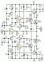
Offset is adjusted with R42
Quiescence-current (50mA) with R43.
To get thermal compensation I put Q9 + Q11 in thermal contact
with the cooler.
The compensation depends from the relationship of R27 to the sum of R32/33 and for the other side from R18 to R36/37. This and the current through R44/43 and R42 gives in my simulation a (small) temperature-overcompensation when I look only to the chip-temps, but in reality of course the cooler-temperature is less.
This "clone" works quite fine (in simu!) especially when I think to the low BOM!
Most things about the (good) propertys I could reed in this thread I can find also in my simulations!
So I think this circuit (Gregs S.K.A.!) looks simple and easy to construct!
If I will do this, of course I will go the easiest way :
I buy it from the Guru!
There is only one thing that puzzled me:
The powersupply-rejection in my circuit is only -43dB (10kHz) and not about -70dB as I can see in Greg`s pic!
I test it in AC- and Tran-Analyse.
When I cut out C12/13 it`s even a little better.
BTW as Greg pointed out in this case thd (10kHz)
rises from 0.025 to 0.5%).
Greg, do you find in my "clone" some of your claims?
Regards
Heinz!
again it`s me
Because I don`t get satisfying info about Your other claims and I also just don`t have US$54 in my bag I must think for myself and guess!
..."There are some 7 claims in the patent application covering the
bias adjustment, DC offset adjust and thermal compensation."..
On my old EWB I have done a few simulations with my
S.K.A.-clon!
(Clon is actual the wrong word for this because clon means exactly the same thing!)
Offset is adjusted with R42
Quiescence-current (50mA) with R43.
To get thermal compensation I put Q9 + Q11 in thermal contact
with the cooler.
The compensation depends from the relationship of R27 to the sum of R32/33 and for the other side from R18 to R36/37. This and the current through R44/43 and R42 gives in my simulation a (small) temperature-overcompensation when I look only to the chip-temps, but in reality of course the cooler-temperature is less.
This "clone" works quite fine (in simu!) especially when I think to the low BOM!
Most things about the (good) propertys I could reed in this thread I can find also in my simulations!
So I think this circuit (Gregs S.K.A.!) looks simple and easy to construct!
If I will do this, of course I will go the easiest way :
I buy it from the Guru!
There is only one thing that puzzled me:
The powersupply-rejection in my circuit is only -43dB (10kHz) and not about -70dB as I can see in Greg`s pic!
I test it in AC- and Tran-Analyse.
When I cut out C12/13 it`s even a little better.
BTW as Greg pointed out in this case thd (10kHz)
rises from 0.025 to 0.5%).
Greg, do you find in my "clone" some of your claims?
Regards
Heinz!
Attachments
Hi Heinz,
Excellent sleuthing there. Quite close ! However I'm using BC546/56C's for low bias current and current sources are 1mA. I have a slightly more complex current source arrangement as Tcomp is too severe as your cct stands ( about 1/2 is required).
Q12 and Q13 loads should be joined and floated from ground, giving a push/pull complementary EF. That may help the PSRR sim.
But you're so close I can't comment further I need some proprietary detail. By the way, your sim will burn test resistors with a switch on surge. Mine doesn't.
I'm happy with Vgs matching of these MOSFETs as they have an inherent source R with a +ve tempco.
Glad you like it.
Cheers,
Greg
I could go on about high feedback ground currents from the inner loop or clipping behaviour with that chip shooting to +/- 14V into that diff'l stage. But I won't.
...pity .
Heinz wrote:
Greg wrote:
http://www.diyaudio.com/forums/attachment.php?s=&postid=750660&stamp=1130113225
Heinz, please, check the open loop gain of S.K.A.1?
please show the simulation plots.
There is only one thing that puzzled me: The power supply-rejection in my circuit is only -43dB (10kHz) and not about -70dB as I can see in Greg`s pic!
Greg wrote:
80dB (gain) in the bootstrapped first stage and 30dB in the output stage with a two pole response from 100KHz due to the output stage and a feedback zero to compensate. with the bootstrap C's removed - this drops the first stage gain by 40dB
EF interposed really did the trick, I was able to use it for bootstrapping, resulting in the really high first stage gain and linearity. If I take out the bootstrap C'c it still functions but THD goes up over 50 times to about 0.25%, the diff'l stage being near it's 70mV input limit (52mV + Vre)
current sources are 1mA
http://www.diyaudio.com/forums/attachment.php?s=&postid=750660&stamp=1130113225
Heinz, please, check the open loop gain of S.K.A.1?
please show the simulation plots.
Hi Heinz,
Your sim would also benefit from proper characterisation of the BC546C/56C's which I had to do from splicing the spice for BC547C/57C's with BC546B/56B's as they were not available. I then adjusted them for the typical Hfe I have in the shipload of devices I have here. The vast majority of BC546C's having 500 <Hfe < 550 while BC556C's had 450 <Hfe< 500 mostly.
Also The IRFPs are 240/9240 so you will need their spice and forget the tempco, you won't find that. I jigged and measured 100 pairs of them.
Hi Jam,
I do not include the input film capacitor as it's not needed now. The bias currents for the input stage after subtraction are roughly 10-15% of Ib for the BC556 i.e -ve at the bases and FB point. at Ic =500uA , hfe = 500, diff in Ib = 15%Ib = .15uA. through27K gives Voffset = 4mV so no need. The inbuilt offset adjustment has a range of 100mV or more. that eliminates one film C which tend to pick up hum at LF and are only as good as the film.
However I did make provision for it in case someone has DC from their source they can't eliminate otherwise.
Hi Dimitri,
nothing to answer. Pls email me.
Hi mikelm,
100dB
The CCS's are 1mA and not adjustable as it would be very fiddly to do bias and offset this way. Just the temp comp.
Cheers,
greg
Hi Jam,
Sorry I missed your question there. The input stage could use JFETs biassed from the CCS's, I just haven't tried it. However it was certainly considered an option and still is - you would need to source something like 2SK389/J109's in the same grading - a worthwhile exercise.
The bias and offset adjustments are achieved in a simple and elegant fashion which is shown on the schematic. Not in the current sources.
Cheers,
Greg
OK... So what are you going to fuel with this?
Its a High output voltage amp.
I don't think you are going to drive any loudspeaker with this amplifier, not with 10 Ohm Source resistors in the output
MTP2N50E.,MOTOROLA TMOS POWER FET 2.0 AMPERES 500 VOLTS RDS(on) = 3.6 Ohms
No I think so.... could make a very interesting head phone amp though

LOL:
Its a High output voltage amp.
I don't think you are going to drive any loudspeaker with this amplifier, not with 10 Ohm Source resistors in the output
MTP2N50E.,MOTOROLA TMOS POWER FET 2.0 AMPERES 500 VOLTS RDS(on) = 3.6 Ohms
No I think so.... could make a very interesting head phone amp though
LOL:
- Status
- Not open for further replies.
- Home
- Amplifiers
- Solid State
- Simple Killer Amp!