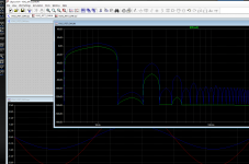
I did the simulation:
I attach photo of FFT.
bias needed is around +1.65V
Circuit is far from tuned because KP1 seems better fit for negative bias. So needs a lot of tuning and now I manage only 3.5 App. With SiCs I manage 7App
It needs more work and I have to stop again working due to other obligations.
I attach photo of FFT.
bias needed is around +1.65V
Circuit is far from tuned because KP1 seems better fit for negative bias. So needs a lot of tuning and now I manage only 3.5 App. With SiCs I manage 7App
It needs more work and I have to stop again working due to other obligations.
Attachments
Circuit is far from tuned because KP1 seems better fit for negative bias.
On J111 (Idss-100 mA), the optimal offset is + 1 ... 2 V. For SiC, use J112 (Idss-50 mA). The maximum amplitude of the offset depends on the Idss Jfet, which are in the buffer. As the Idss increases, the offset shifts towards the positive side. When decreasing - in the negative direction. This must be taken into account in the simulator.
Correct. For this simulation I used J111 but the problem is not the bias, I manage to get it correctly, no issue there. The problem is the amplitude of the driving signal of the final stage FETs. Without much tuning I get 30 Vpp, which on 8 Ohm gives me 3.5 App.
With SiCs but with a lot of tuning I had doubled that.
BTW the input signal is 0.3Vpp which makes this design proper for FULL integrated amplifier, not final stage, with only two stages!!! Excellent design!!!
Still, haven't managed to create the prototype, even if I have soldered the PCBs and have all the parts in place... But I am close...
OK using 2N4091 i can get 4App. In general it needs work to go up. The final stage I use is GS66508. They seem to work excellent. I get for now to 0.05THD in 4W but mainly due to buffer stage not the final stage.
Last edited:
But I am close...
It would be very good if you further improve this KP1 circuit.
 I do not know how to work on simulators. I'm more used to working with a soldering iron.
 For an open-loop circlotron, high power and low output impedance Rout can be obtained only with high Qfs field-effect Mosfet transistors.
Last edited:
")
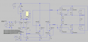
the circuit is good for 100W RMS
It is the circuit I have already soldered but not put in the case....
Great job !!!


But you need to swap J1 and J2. J1: Idss - 10 .... 20 mA, J2: Idss - 3 .... 5 mA. 2N4416: Idss - 5-15 mA.
The stable current generator circuit has been modified and may be unstable.
Last edited:
Thanx. I had it that way and couldn't make the circuit stable... Any way let me try again
PS. Did it, same results but it takes longer to analyze circuit: J1: 37mW, J2: 3mW
OK, now I remember why I had reverted them. The correct way gives me a little worse distortion (a little bigger 3rd harmonic)
PS. Did it, same results but it takes longer to analyze circuit: J1: 37mW, J2: 3mW
OK, now I remember why I had reverted them. The correct way gives me a little worse distortion (a little bigger 3rd harmonic)
Last edited:
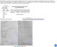
On a Russian forum, author Sergei (Svjatoslav) investigated a stable current generator(SCG):"I examined the cascode SCG for current stability, depending on the voltage drop across it (see table).
It can be seen that the circuit reliably generates a stable current at a voltage of 3.5 V and above, providing an internal resistance greater than that of a bipolar transistor circuit."
This circuit is very stable, provided that J1 is Idss = 10 ... 20 mA, J2 is 3 ... 5 mA.
It can be seen that the circuit reliably generates a stable current at a voltage of 3.5 V and above, providing an internal resistance greater than that of a bipolar transistor circuit."
This circuit is very stable, provided that J1 is Idss = 10 ... 20 mA, J2 is 3 ... 5 mA.
Attachments
Last edited:
Jpatay,
this is one of the most intriguing designs out there so I am going to embark in this.
I was able to source all the jfets exactly as shown in schematic. Can you confirm the circuit in post #27 is the correct schematic to use for the 2sJ103/246, the J112 and the UJ3 SiC Jfets?
I am not clear if there is a PCBWay PCB done for it and(or) an available power supply board for it.
I would also like to know what is the power output and the quiescent current as drawn in post #27 just to make sure I get the heat sinks sized adequately.
Thanks
Yes, the circuit from post # 27 will do. Instead of 2SJ103Y (VT3, VT4), you can use 2SJ103GR. On VT5, VT6, you can put J175 (Idss-25 mA). Quiescent current - 0.3 ... 0.4 A.
In the post # 199, 200 there is some information.
The boards can be ordered here:
JFET-only Circlotrons without NFB v2 - Share Project - PCBWay
Power supply unit for JFET-only Circlotron - Share Project - PCBWay
The maximum power into a load of 8 ohms is 50 watts. I don't remember exactly, but it seems the maximum amplitude was 20 V.
For SiC, you will have to install a temperature sensor on the heatsink. And provide SiC power-on delay.
Last edited:
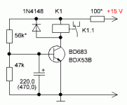
Protection board:
Simple Speaker Turn-On Delay and DC Protector - Share Project - PCBWay
Simple Speaker Turn-On Delay and DC Protector - Share Project - PCBWay
Thanks, I have both 103GR and Y.
50W is more than plenty!
What kinds of J112 or J175 fets are people buying? Mouser has interFET or ON semi. The former much more $$$. Do you know why that is?
Another question: is this suitable to operate with balanced input from the differential input?
I was wondering about the SiC normally closed operation what happens at startup...what kind of power on delay and temp sensor are people using? Do you have some suggestions or links?
Thanks!
PS I just saw you sent some info as I was writing.
I bought cheap J112s. I don't know who the manufacturer is. On them there is such an inscription: WJ38 J112.
The balanced input works, but I liked the line input better.
I used a protection board for the SiC power-on delay.
For a temperature sensor, you can use 2-3 pieces of silicon transistors, but use them as diodes. Connect B and K together.
The sensor is shown in the circuit in post 200.
The balanced input works, but I liked the line input better.
I used a protection board for the SiC power-on delay.
For a temperature sensor, you can use 2-3 pieces of silicon transistors, but use them as diodes. Connect B and K together.
The sensor is shown in the circuit in post 200.
I saw the circuit with the thermosensor installed post #200.
What is that? It's in russian.
Yes, these are Russian germanium diodes. You can use silicon diodes, but you have to experiment.
I was wondering about the SiC normally closed operation what happens at startup...
UJ3N065080K3S will be closed provided that the gate is -12 V or more. When the amplifier is turned on, the SiC will be open until a negative voltage appears at the gate. To prevent the fuses from blowing, it is necessary to delay the power supply to the SiC for 2 seconds until -8.5 V appears on the gates. To do this, you can use a protection board to supply AC voltage to the primary winding of the power transformer.
Attachments
yes ok so you need the neg vgs to bring the resistance up so as to flow the correct 400mA bias.
Yes. And for a quiescent current of 400 mA, the offset is approximately -8.8 V.
As the negative bias across the SiC gates increases, the quiescent current will decrease.
Last edited:
- Home
- Amplifiers
- Solid State
- JFET-only Circlotrons without negative feedback