It is very good that the work is progressing. There is never enough time, but there is always time for hobbies. 😉
Access to this page has been denied. (GS66508T-MR)
these GAN system mosfets are even better than any SIC in all aspects
You should try it. Also you should use SIC diodes at least in high current part. Silicon transistors, diodes are too slow.
Bias it @ 1,2-1,4A R12,13 resistors should be 50-80R 0,1% mills non inductive, not 200R
these GAN system mosfets are even better than any SIC in all aspects
You should try it. Also you should use SIC diodes at least in high current part. Silicon transistors, diodes are too slow.
Bias it @ 1,2-1,4A R12,13 resistors should be 50-80R 0,1% mills non inductive, not 200R
Last edited:
There is a desire to make a powerful amplifier exclusively on JFET.
Without negative feedback.
Tested circuit at low power is already available.
There is now a powerful MOSFET output scheme.
The next step - a powerful circuit Si-C JFET.
Related topic:
JFET-only Headphone Amp "Circlotron КП903B".
Svjatoslav, have you tried lu1014d in your circuit?
Unfortunately, I did not try to use it.
It looks like it can be used in KP1.
But in the passport its characteristic is very inconvenient. Not what is needed, the range of currents and voltages.
It looks like it can be used in KP1.
But in the passport its characteristic is very inconvenient. Not what is needed, the range of currents and voltages.
Access to this page has been denied. (GS66508T-MR)
these GAN system mosfets are even better than any SIC in all aspects
You should try it. Also you should use SIC diodes at least in high current part. Silicon transistors, diodes are too slow.
Bias it @ 1,2-1,4A R12,13 resistors should be 50-80R 0,1% mills non inductive, not 200R
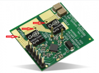
Very interesting devices. However very difficult to handle due to package. Simulation shows great results.
have you tried lu1014d in your circuit?
These transistors are very difficult to find. They were installed in older computers.
Very interesting devices. However very difficult to handle due to package. Simulation shows great results.
The price is also good. 🙂
Yes it's rather expensive but in test simulation circuit gave me ten times lower distortion than SICs. Still, I don't understand how to effectively mount them on a heatsink. Read the application note which was confusing.
Still, I don't understand how to effectively mount them on a heatsink. Read the application note which was confusing.
If you look at the finished product, then you need to solder the GAN to the board, and then attach the board to the radiator.
Attachments
(The GS61004B is a bottom-cooled transistor that offer very low junction-to-case thermal resistance for demanding high power applications. These features combine to provide very high efficiency power switching.)
There is also a GAN GS61004B for 100 V. We don't need 650 V.
https://gansystems.com/wp-content/uploads/2018/04/GS61004B-DS-Rev-180419.pdf
It is necessary to study their parameters well.
There is also a GAN GS61004B for 100 V. We don't need 650 V.
https://gansystems.com/wp-content/uploads/2018/04/GS61004B-DS-Rev-180419.pdf
It is necessary to study their parameters well.
Yes, I read very carefully the application note but I had never used that before and it puzzles me about how efficient it will be. Also all application notes are about SMPS and Digital amplifiers that don't have really much need for cooling.
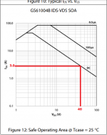
With lower voltage and power variants what worries me is the safe operating area. For example for 61004 if you have Vds=40V then you can go upto 2.5A. What is your opinion, because many times I choose FETs based on SOA and I end up with high power and voltage variants.
With lower voltage and power variants what worries me is the safe operating area. For example for 61004 if you have Vds=40V then you can go upto 2.5A. What is your opinion, because many times I choose FETs based on SOA and I end up with high power and voltage variants.
the BEST solution is to make bare 2mm copper pad. Other solution is to buy different package GS66508B-MR GaN Systems | Mouser Europe and to make aluminum substrate pcb. GAN GS61004B for 100 V will work safely until 30V@1,2A. 45V@1,2A might be too dangerous
Attachments
Last edited:
With lower voltage and power variants what worries me is the safe operating area. For example for 61004 if you have Vds=40V then you can go upto 2.5A. What is your opinion, because many times I choose FETs based on SOA and I end up with high power and voltage variants.
If you look at the graph, then with a power supply of 40 V, the maximum current is 3 A. This is at +25 ° C.
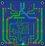
For this circuit KP1, these transistors should fit. It is not known what maximum power can be obtained with these transistors according to the KP1 circuit. And what is the output impedance of the amplifier.
Attachments
and to make aluminum substrate pcb.
 This aluminum PCB is very good.
Hmm so even lower from what I suggested. So we need another FET and for sure I need something with higher power for another application. In any case, I am considering the options, because distortion numbers from simulation were very promising...the BEST solution is to make bare 2mm copper pad. Other solution is to buy different package GS66508B-MR GaN Systems | Mouser Europe and to make aluminum substrate pcb. GAN GS61004B for 100 V will work safely until 30V@1,2A. 45V@1,2A might be too dangerous
Levelup says much lower and don't expect these to work at 25C, i believe much more. So we need a more powerful but I see we agree for SOA consideration. Which schematic is the KP1?If you look at the graph, then with a power supply of 40 V, the maximum current is 3 A. This is at +25 ° C.
For this circuit KP1, these transistors should fit. It is not known what maximum power can be obtained with these transistors according to the KP1 circuit. And what is the output impedance of the amplifier.
This one is from the first post.Which schematic is the KP1?
I have not found analog amplifier circuits made on the GAN.
Attachments

They don't have analog, that's why I worry. The digital applications they have do not produce much heat. On their big digital amplifier they don't have cooling at all. I read many application notes and they had on note that dissipation would be about 30W max and that was on their big FET, which is far from what I use, because I run my amplifiers hot.
The less than 1cm2 they have seems to me too little to stand big loads.
The KP1 bias voltage seems right.
For now the simulation I had run was on Class A, not circlotron. I will put it on circlotron simulation and see what happens.
The less than 1cm2 they have seems to me too little to stand big loads.
The KP1 bias voltage seems right.
For now the simulation I had run was on Class A, not circlotron. I will put it on circlotron simulation and see what happens.
I will put it on circlotron simulation and see what happens.
OK.
- Home
- Amplifiers
- Solid State
- JFET-only Circlotrons without negative feedback