Mark, IMO whatever anyone has to share with others about USB to I2S converters (not only measurements), better be on a dedicated thread. Otherwise info is lost when spread over on DAC threads.
George
George
Wires between the USB board and the dac board are pretty long, and not even signal wires loosely twisted with individual dedicated ground wires. Not ideal.
Better clocks should help reproduction quality. JL sounds makes a very good one which is called I2SoverUSB. Many people say it is the best sounding USB board they have tried. Clocks are NDK SDA, and the board is galvanically isolated from USB power and ground. I2SoverUSB - I2S over USB Audio
I have the "i2SoverUSB" Audio board, though haven't tried it. From my understanding of the way this board works, the asynchronous XMOS based device (being jittery and noisy to whatever degree) is separated by galvanic isolators to the secondary. The two "reference" crystals are on the secondary (clean?) side of the galvanic isolators, with the crystal clock signals being passed back through the galvanic isolators to control the timing of the XMOS chip.
The data output signals from the XMOS can be argued to still contain questionably high levels of objectionable noise by virtue of extensive high frequency signal processing, etc., however these lines have been time referenced to the reference crystal on the secondary side, whereupon a latch is then used from a clean edge of the reference crystal (where data levels are guaranteed stable) to clean up the noisy data signals. The extent these lines are "cleaned" is a function of such factors as the quality of the reference crystals, the galvanic isolation and the quality of the secondary power supplies.
This is to suggest that the reputation of the board can be equated to the excellence in the manner of its implementation.
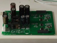
Hi Richard, your dac looks interesting. I like how you’ve made the filtering include a lift at high frequency to compensate for the RBCD droop.
Have you also played with a high order filter without the HF lift, made for higher sampling rates? With say, 88.2k SR the aliasing images would be doubled in frequency, and the 7th order filter would be even more effective at blocking them. I’ve been using Audirvana which allows you to choose the sampling rate sent to the dac.
Have you also played with a high order filter without the HF lift, made for higher sampling rates? With say, 88.2k SR the aliasing images would be doubled in frequency, and the 7th order filter would be even more effective at blocking them. I’ve been using Audirvana which allows you to choose the sampling rate sent to the dac.
Hi Colin - yes I have indeed played with variations on filters. I even put up some simulated responses and measurements for using a passive filter designed for 2XOS : lingDAC - cost effective RBCD multibit DAC design lingDAC - cost effective RBCD multibit DAC design
A bit later on I posted a subjective comparison and found a slight preference for 2XOS.
The 2XOS passive filter is a bit simpler than the NOS filter as its a traditional Chebyshev with no stop-band zeros. This saves on a few RC networks. The droop correction is done in the final stage active filtering so running a 2XOS filter needs some component value tweaks to that filter (the one built around AD744 in the schematic). I will look at my notebook and sims to get back to you on the changes to component values.
Nice one, thankyou. Being in the final filter stage makes things easier to implement. I’m thinking of using relays to switch between the filters automatically with sampling rate.

Fabulous, thankyou! It could be good if you‘d make that available as a ‘hat’ for the PhiDac as well.
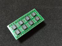
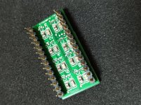
Single chip test DAC
Seeing as I've run into one or two cases where DACs have given out strange noises at low levels and the usual test of checking pin7 voltage hasn't revealed an obvious problem I decided to build a board which will allow me to listen to a single DAC chip at a time, in a ZIF test socket.
The schematic is based on PhiDAC hex but instead of level shifting the logic signals to the DAC chip I decided to play with level shifting the outputs. That seems to work quite well - just zener diodes biassed by current sources brings the DAC output compliance range up to half the analog supply - which in this case is 24V.
The filter board isn't a normal PhiDAC hex filter - I built a custom one with higher impedance (240ohm rather than 47ohm). The shocker when I listened was that this DAC sounds much more like 'hex' than the original PhiDAC in that it fills in the low-level ambience which original PhiDAC loses. Since I had originally put the extra ambience of 'hex' (and GrossDAC) down to having many paralleled DAC chips this came as something of a surprise. How can a single chip get down to the lower effective noise levels of the paralleled DACs?
Based on further experiments seems the answer to this is in the I/V stage. It's that that's too noisy in original PhiDAC. Putting more DACs in front of the I/V opamp increases the signal while keeping the noise the same. Hence better SNR. A higher impedance filter results in less noise by virtue of lowering the noise gain of the I/V.
This little nugget of understanding inclines me to revisit the original PhiDAC and see if there's any way I can fix up its lack of low-level details while sticking with its single DAC chip, single PCB format....
Attachments
Based on further experiments seems the answer to this is in the I/V stage. It's that that's too noisy in original PhiDAC. Putting more DACs in front of the I/V opamp increases the signal while keeping the noise the same. Hence better SNR. A higher impedance filter results in less noise by virtue of lowering the noise gain of the I/V.
Maybe independently decoupling of single chip in nature? Can you extend your investigation with independently decoupling and bypassing each chip by following a similar layout in photos? The photos are belong to TDA1541 to TDA1387 replacement adapter on Aliexpress.
https://www.edn.com/bypass-or-decouple-your-way-to-power-supply-noise-reduction/
Attachments
Noise gain studies...
Continuing on the topic of noise gain, I had a look at how my AD744 NOS-droop filter behaves noise-wise and figured I can reduce its noise contribution by a few dB by reducing the Q at the expense of FR flatness.
This article shows that Sallen-Key filters are better when low noise is required - because MFB by default has a 6dB noise penalty by virtue of being inverting. However they don't point a crucial upside of MFB - its better OOB performance.
https://e2e.ti.com/blogs_/archives/b/precisionhub/archive/2014/03/24/noise-from-active-filters-an-unwelcome-surprise
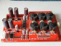
New Phi DAC for 2021
Here's the first prototype Phi DecaDAC - using 10 TDA1387s to improve the SNR downstream. I'm estimating about 12dB reduction in the noise by virtue of
1) using more DAC chips hence more signal
2) substituting LT1028 opamps for AD829s in the I/V stage
To ensure the gains in the I/V aren't lost in the EQ stage I've tweaked the noise gain there and exchanged AD744s for an ISL28210.
The AD815 in the power supply has been changed to an LM317 for the opamps and a discrete darlington for the DAC chips.
Schematic to follow later this week.
Attachments

LM317 for the opamps and a discrete darlington for the DAC chips.
You could implement Elvee's denoiser with no cost.
LV's denoiser was one thing I tried during development of this revision. I didn't notice any improvement in SQ so it didn't get included.
Schematic for Phi DecaDAC
I've added one or two more test points to make test and fault-finding a little bit easier compared to the 'hex' and also the voltages expected at those nodes.
Current consumption is a little bit higher than the 'hex' - whilst I've saved on the not-insignificant quiescent of the AD815, the extra 4 DAC chips more than cancel that saving out.
Attachments
Great, highly appreciated.
You use TL431 for GND (4,54V) supply of TDA1387.
Would an additional capacitor decrease noise of TL431 by arround 10dB?
C2 in figure 1(c) TL431 notes.
You use TL431 for GND (4,54V) supply of TDA1387.
Would an additional capacitor decrease noise of TL431 by arround 10dB?
C2 in figure 1(c) TL431 notes.
- Home
- Source & Line
- Digital Line Level
- lingDAC - cost effective RBCD multibit DAC design