I would surface mount opamps. Some people feel the best of leaded components still sound better than SMD versions, but there are said to be some good little glass cylinder MELF SMD resistor types.
I assume you mean use the surface mount op amp part number, not the surface mount sockets that hold DIP versions of the op amps? I could use surface mount sockets so that I could swap op amps but not have the swiss cheese ground plane. Some of the surface mount sockets that are sold look just like through hole machine screw sockets but without the pins.
By the time I try making a PCB I might have already narrowed down the op amp choice anyways.
Did you reconfigure the I2C library settings to use the correct I2C pins/port for Due?
Hmm, no..in wire.h?
Kozard: Thanks for the idé, i have tried both 3.3 and 5v. No diffrent.
BR // Daniel
Last edited:
kozard,
If you want to use sockets then it gets a little messy. OPA1612 is an SMD part, so it would have to be on a dip adapter to plug into a socket. Put an SMD socket under the DIP adapter and pretty soon you have a stack of stuff sticking up off the board. More lead inductance, less proximity to the ground plane, etc. If its a must have, one could do it of course. Probably better just to learn SMD hand soldering and learn how to remove and replace opamps if necessary, or maybe if you want to try OPA1656. At least that one might be a viable choice. 5532 is pretty much a waste of time. Time that could be more productively spent elsewhere.
If you want to use sockets then it gets a little messy. OPA1612 is an SMD part, so it would have to be on a dip adapter to plug into a socket. Put an SMD socket under the DIP adapter and pretty soon you have a stack of stuff sticking up off the board. More lead inductance, less proximity to the ground plane, etc. If its a must have, one could do it of course. Probably better just to learn SMD hand soldering and learn how to remove and replace opamps if necessary, or maybe if you want to try OPA1656. At least that one might be a viable choice. 5532 is pretty much a waste of time. Time that could be more productively spent elsewhere.
Daniel,
I you have a scope you can look at the I2C bus signals and see if they pulled up to 3.3v when idle. When you send an I2C command you should see nice square waves briefly on SCL and SCA. You may have to set the scope to trigger in single sweep mode in order to catch the brief pulse train. If the square waves are slow to rise back up to 3.3v on their trailing edges, then your pullups are probably too high resistance. Also, it will be a hardware check to make sure software is working right.
Regarding how to set the correct I2C pins for Due, it depends on which I2C library you are using. If using the built-in Wire library that data may automatically be configured. If using the library I used then there are some statements at the beginning of the program to configure the I2C pins that go (IIRC) before the library include statement. Its all explained the .md file for the library.
EDIT: Also, I think we talked before about getting pinout diagram for the Arduino you are using. That shows which are the hardware I2C pins and what I/O 'port' they are on.
Last edited:
Thanks Mark, for now i use wire. Can try the one you use in your perfect Reg editor to see if a can ”catch” the EEPROM then.
I use pin 20 and 21 in Due. I read that it has a second i2c line. Should try that one also to see if it works.
BR // Daniel
I use pin 20 and 21 in Due. I read that it has a second i2c line. Should try that one also to see if it works.
BR // Daniel
Solved! Two days of trial and error and some bad words all because I solder my two i2c wires to the wrong scl and sda (70,71)..i mixed up 70,71 and 20,21..
Now settings are saved..
BR // Daniel
Now settings are saved..
BR // Daniel
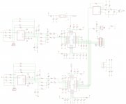
Someone posted this as the schematic. (Attached.)
If you just got the board be aware that the output stage needs to be replaced with an I/V stage. I mean it really needs to be replaced.
Thank you for the schematic. I made a few changes.
-replaced NE5532 to LME49720
-desoldered output coupling caps C17 and C30
-removed R10 and R25
-R7 and R22 decreased to 10ohm
I measuring some DC offset (+100mV...+200mV) in OPA output pins in dual supply mode. R26 R28 voltage divider is unimportant in dual supply mode but the common point of R27 R11 must be bound to GND in my oppinion. I will try this. Which of the output stage is recommended to build? This? https://www.diyaudio.com/forums/digital-line-level/314935-es9038q2m-board-301.html#post5577605
I have not built that one (#3003) but others have and recommend it.
I have built the one in post #6944.
In post #6981 I have included measurements of mine (prototype board only). When I start to change component values (R1, C1 in I/V) toward that of post #3003 my THD degrades about 10 dB. Note that this is in a prototype environment only. No new PCB. I also wonder if I am at the limits of my Creative Professional/E-MU 1820 for measurements.
If you try 3003 could you measure your THD/spectrum and post it? (Before and after the modifications?) (If you are able to.) Recommend measuring with 32 averages, 1M point FFT and both with and without coherent averages. (If you are using REW that is. With "display distortion" turned on.)
Last edited:
I measuring some DC offset (+100mV...+200mV) in OPA output pins in dual supply mode. R26 R28 voltage divider is unimportant in dual supply mode but the common point of R27 R11 must be bound to GND in my oppinion. I will try this. Which of the output stage is recommended to build? This? https://www.diyaudio.com/forums/digital-line-level/314935-es9038q2m-board-301.html#post5577605
I soldered a copper wire shunt across C32 and another across C34.
The virtual ground offset generator is not needed for dual supply operation (only for single supply operation). It also grounds one half of each output network to a different ground (the virtual ground) instead of the ground plane. I am not sure that is a great idea for noise.
But if the power supply is not completely symmetrical for example +15.05V -14.95V then an offset will appear on the output in virtual GND mode. Can be fine-tuned by changing the value of the voltage divider with 25 turn trimmer.
Although the voltage divider can be tweaked to remove DC offset its probably better to bypass the capacitors used to provide an AC ground, as kozard suggested. The caps aren't needed when running from dual supplies and given their nonlinearity they can't be doing anything to help the sound. (Not that a voltage mode output stage will ever sound very good, of course.)
There you go with them blanket statements again.(Not that a voltage mode output stage will ever sound very good, of course.)
The imbalance between -/+ power supplies (ie. the common mode output voltage) only matters if you are swinging close to the rails though, surely? As long as the rail to rail output swing spec for the chosen opamp is within range, it will be AOK.
My plan: Dual mono ES9039Q2M. Power supply (not shown) will use 3x discrete shunt 3.3V. My PSU was not tested yet. But I have made +-15VDC and 5VDC discrete shunt regulator. Basic shunt regulator from Walt Jung (he used op-amp).
What are R26/C24 and the likes here for? It looks like you're trying to do passive RC filtering before the I/V stage - won't that mess up the virtual ground that the DAC output wants to see?
Hi Bimo,
Don't know what experience you have with ES9038Q2M. When I look at your schematic I see many problems that can be expected to adversely affect measured and audible performance. Not sure if you posted the schematic to get feedback from us, or you just want to share? If you want feedback, I'm sure some of us would be happy comment.
Best,
Mark
Hi Bimo,
Don't know what experience you have with ES9038Q2M. When I look at your schematic I see many problems that can be expected to adversely affect measured and audible performance. Not sure if you posted the schematic to get feedback from us, or you just want to share? If you want feedback, I'm sure some of us would be happy comment.
Best,
Mark
Why did you think there is a problem? Where are the problem?
I do not have experience in DAC, but I have experience in embedded engineering and I have design many amplifiers, some of them cheap and others can defeat commercial product which much more expensive according to local audio community here.
for starters, as mentioned above by TFive, you appear to be designing a voltage buffer, rather than an I/V convertor. this lowers objective performance considerably with ESS. either perform the filtering within the local NFB loop of the I/V opamp, or between 1st and second stage opamps; but whatever you do, dont do it as you have now. Ideally the DAC outputs should be driving the inverting opamp inputs directly.
Hi Bimo,
There is a pretty good paper that ESS published before they decided to go NDA (more recently, they decided to lift most of the NDA secrecy). Its available on their website: http://www.esstech.com/index.php/download_file/view/69/267/ ...Highly recommend it for careful study to start with. Not just the schematics either, all of the text is important to keep in mind.
Also, something I can post now is the schematic for ES9038PRO evaluation board (attached below). Regarding it, I'm not sure I would do everything just like they do because I don't think its the way to get the best sound out of their chips. I'm just sharing it as a point of reference to start with.
In addition there are some schematics attached to post #3003 of this thread that may be worth taking a look at.
When you are ready we can talk in a lot more detail about options for a really good ES9038Q2M dac design that you could hopefully be happy with.
EDIT: Sorry, was so focused on trying to think of how to start explaining, that I missed replying directly to your question regarding issues in the schematic you posted. I can't think of a great way to say this, but in my view there are more things that are problems than their are things that are right. It feels too soon to take them one by one, maybe better if we can get you thinking in a somewhat different way about these dac chips first.
Attachments
Last edited:
- Home
- Source & Line
- Digital Line Level
- ES9038Q2M Board