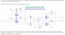
On the subject of leaving two output stages connected to the dac outputs at once, I would at least suggest to remove any opamps from their sockets that are not needed when using an alternate output stage. Also, there may be some small, or even not so small audible effects from leaving unneeded passive components in a circuit. Although I/V opamps hold the dac outputs at AVCC/2 volts at least to a first approximation, they do allow some voltage swing. Otherwise, if you put a small cap to ground at an I/V input it would have no effect at all because there is only DC voltage across it. In reality, it will cause gain peaking in the opamp (which is not a desirable thing).
I just fired up my prototype of the "ES9038Q2M No Hump IV Output Stage" From Post 6944.
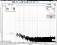
For this first test I am using the JRC 4580D and I pretty impressed at this modest op-amp. The 2.2nF are polyester film capacitors and the 220pF are 3kV blue ceramic capacitors. I need to place an order for Wima foil capacitors in these values.
The attached results are (in order):
1. Loopback test of E-MU 1820 at the same input power (due to noise questions).
2. -20 dBFS
3. -10 dBFS
4. 0.0 dBFS
5. Schematic
Attachments
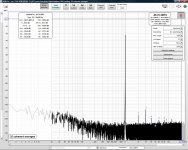
Now using the ST LM833N here are my results from my first tests of my prototype of the "ES9038Q2M No Hump IV Output Stage" From Post 6944.
The 2.2nF are polyester film capacitors and the 220pF are 3kV blue ceramic capacitors. I need to place an order for Wima foil capacitors in these values.
The attached results are (in order):
1. Loopback test of E-MU 1820 at the same input power (due to noise questions).
2. -20 dBFS
3. -10 dBFS
4. 0.0 dBFS
5. Schematic
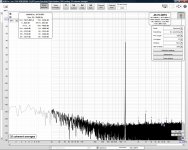
Attachments


Have you calibrated the REW levels with E-MU1820? I would expect FS to be much more than 1 Vrms. Also your DAC output seems quite low if you have only -16.7 dbFS at 0 dBFS input (with FS being 1 Vrms).
I just got the E-MU 1820 working again on Tuesday (after a number of years not being used) and I have not calibrated it yet in REW. I can look at that tomorrow.
I am displaying in dBFS (uncalibrated) which is dB from full scale on the E-MU. The E-MU 1820 is setup in patchmix for +4dBu levels. (Professional audio levels.) Also the Mic A input (on the E-MU 1820) is set to minimum gain.
Also that output stage from post 6944 is using 390 Ohm resistors in the IV. So doesn't that limit the output voltage also? (Considering the output current from the ES9038Q2M?)
I should also note that this is single ended right now. I built a balanced IV stage but I am only looking at one side. I will later build the XLR cable for the prototype. I started with single ended cables because my test amplifier is single ended.
Have you calibrated the REW levels with E-MU1820? I would expect FS to be much more than 1 Vrms. Also your DAC output seems quite low if you have only -16.7 dbFS at 0 dBFS input (with FS being 1 Vrms).
All of this is with the EMU 1820 set to +4 dBu (professional) levels:
With full scale output of the EMU 1820 I read 3.980Vrms output of the EMU 1820 (1L Output). Looping back into the Mic A (gain set to min) input of the EMU 1820 that reads -6.03 dBFS.
Since -6.03 dB is Av=0.499459 that means the full scale on the graphs is =3.980Vrms/0.499459 = 7.968Vrms.
Since -6.03 dB is Av=0.499459 that means the full scale on the graphs is =3.980Vrms/0.499459 = 7.968Vrms.
If I loopback from 1L (output) to 1L (line in) it reads -8.61 dBFS. Since -8.61 dB is Av=0.371108 that means the full scale (if I use that input) is =3.980Vrms/0.371108=10.72Vrms.
So the fullscale levels are pretty high when the +4dBu setting is used on the 1820. (When the EMU 1820 is set from -10 to +4 you can hear relays clicking inside.)
If you see any mistakes please let me know!
Hooking up the DAC again I read 1.20Vrms for full scale with the 390Ohm resistors in the IV stage.
Last edited:
The analog line inputs on the back panel of E-MU 1820 are probably better for measurements (lower noise + THD).
May I ask, did You try to load the apposite RMAA configuration settings when setting up?
That, and setting everything to +4dBu (LINE OUT /IN), and doing a loopback - if the balanced cable is good, one should read back 0dBFS with dac at FS..
One line contact error results in -6dB reading ..
All monitor levels (insert and main) should be at 0dB..
Ciao, George
That, and setting everything to +4dBu (LINE OUT /IN), and doing a loopback - if the balanced cable is good, one should read back 0dBFS with dac at FS..
One line contact error results in -6dB reading ..
All monitor levels (insert and main) should be at 0dB..
Ciao, George
The analog line inputs on the back panel of E-MU 1820 are probably better for measurements (lower noise + THD).
Yes, I am trying that right now. However 0 dBFS seems to overload something on those inputs but not the front inputs.
I might need to do measurements at -3dBFS or something like that.
May I ask, did You try to load the apposite RMAA configuration settings when setting up?
That, and setting everything to +4dBu (LINE OUT /IN), and doing a loopback - if the balanced cable is good, one should read back 0dBFS with dac at FS..
One line contact error results in -6dB reading ..
All monitor levels (insert and main) should be at 0dB..
Ciao, George
I am using one side of the IV output (single ended) and all single ended cables. Hence -6 dB.
Later I can look at balanced. I setup with single ended cables on the IV prototype since my test amplifier is single ended.
Ah ok, I was also thinking of that (that You test single ended..) - but then You had shown a differential I/V output..
Yes, I built the balanced IV that I showed. However I am only testing half (from the positive ouput to ground).
Since there is an offset voltage at the I/V outputs, are you using a DC blocking cap, or does the EMU have one inside it (that would not be operating as a reversed biased electrolytic)?
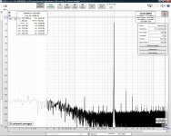
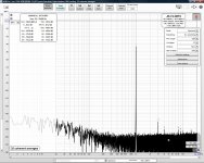
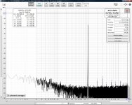
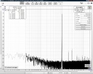
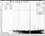
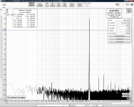
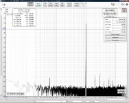
Here are some more measurements made this time with the lower distortion/noise line in (1L) on the back of the EMU 1820. The DAC is at -3.0 dBFS because something overloads in the EMU 1820 around -1.0 dBFS.
These are with my prototype of the "ES9038Q2M No Hump IV Output Stage" From Post 6944. That is a balanced output but I am currently measuring only "half" or the positive output only.
These are measurements again with the JRC4580D op amp.
Attached in order:
Before I try my last op-amps (LM4562, JRC4562 and Ti NE5532) does anyone have any component value or component type/quality suggestions?
I don't have many of the capacitor values that I want in foil and film but this is a start for a prototype. I am using standard 1% metal film resistors. Later I can order better components when (and if) I settle on this one.
These are with my prototype of the "ES9038Q2M No Hump IV Output Stage" From Post 6944. That is a balanced output but I am currently measuring only "half" or the positive output only.
These are measurements again with the JRC4580D op amp.
Attached in order:
- No new modifications. Remeasure with different sound interface input.
- Replace 100uF Xicon output block with Nichicon UES 50V 47uF BP
- Replace 220pF 3kV blue ceramic disk in IV with 470pF polyester film
- Replace 470pF polyester film with 2x100pF Wima FKPS2
- Replace Wima with 1000pF Polystyrene (my only value of polystyrene)
Before I try my last op-amps (LM4562, JRC4562 and Ti NE5532) does anyone have any component value or component type/quality suggestions?
I don't have many of the capacitor values that I want in foil and film but this is a start for a prototype. I am using standard 1% metal film resistors. Later I can order better components when (and if) I settle on this one.
Attachments
-
 JRC4580D Red Side to 1L Input 4dBu Levels Coherent -3dBFS.jpg220.5 KB · Views: 273
 -
 JRC4580D Red Side to 1L Input 4dBu Levels Coherent -3dBFS Nichicon Muse.jpg220.8 KB · Views: 278
 -
 JRC4580D Red Side to 1L Input 4dBu Levels Coherent -3dBFS 470pF Polyester.jpg220.5 KB · Views: 261
 -
 JRC4580D Red Side to 1L Input 4dBu Levels Coherent -3dBFS 2x100pF Wima FKPS2.jpg219.7 KB · Views: 264
 -
 JRC4580D Red Side to 1L Input 4dBu Levels Coherent -3dBFS 1000pF Polystyrene.jpg217.9 KB · Views: 261
Last edited:
How is the output stage grounded to the dac ground plain? With a wire?
EDIT: To quote ESS:
"The most important for DAC performance is the ground plane,
it should be as solid as possible with as few traces routed through the ground plane as possible. Any traces
that are routed through the ground plane and block the “line of sight” from the DAC output to the opamp
output stage significantly degrades the output THD. ESS recommends using the evaluation board designs
as a guide for your own PCB layout. Critical PCB layout items:
1.) Make the ground plane as solid as possible. Try to keep all ground connections as short as possible.
Every ground connection should have its own via, do not share vias if possible.
2.) Keep opamp feedback paths as close as possible to the opamp.
3.) Ensure every opamp and DAC has decoupling capacitance on its power supply right next to the power
supply pins.
4.) The audio path between the DAC and the opamp stage should be kept as short and clean as possible.
5.) The audio path after the opamps is not as critical.
6.) Try to keep the digital circuitry away from the analog circuitry"
EDIT 2: To comment on one ESS recommendation, putting the I/V opamps too close to the dac chip increases the chances of unexplained heating in the opamps (presumed by me to be from RF incursion, but not proven). Thus, my example output stage project had a ground plane soldered to the dac ground plane. Dac chip analog output pairs connected to the I/V inputs over twisted-pair wire-wrap wire run along the dac board ground plane. In that layout, no excess heating was noted. Unfortunately, no time domain view of the outputs looking for signs of hump distortion.
Last edited:
Right now it is just a prototype board with four twisted pair connections to the DAC board. I intend to improve that (quite a bit) if I settle on this DAC and make the PCB for this one. The connections are as short as I can make them. Later I guess I can see what creativity is possible with copper foil and thin metal sheets.
So far with all the different op amps I have had no unexplained op-amp heating. The op amps are cool. I am a good distance from the DAC and the connections are twisted pair.
So far with all the different op amps I have had no unexplained op-amp heating. The op amps are cool. I am a good distance from the DAC and the connections are twisted pair.
Last edited:
Since there is an offset voltage at the I/V outputs, are you using a DC blocking cap, or does the EMU have one inside it (that would not be operating as a reversed biased electrolytic)?
I am using a Nichicon UES BP (47uF 50V) for the DC blocking cap. I first tried 100uF 25V Xicon. No difference in my measurements between the two.
- Home
- Source & Line
- Digital Line Level
- ES9038Q2M Board