Continued from my last post. With 100uF Xicon added to DVDD:
Initial Conclusions:
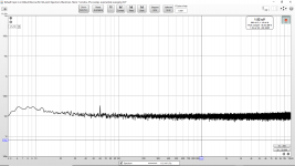
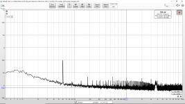
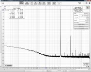
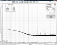
As per the previous measurements the soundcard bandwidth is clearly limited and can not observe RF. That said the ESS demo board schematic has only the same single 1uF ceramic on all five pins, so the present ceramic plus 22uF tantalum on each pin (stock) does not seem abnormal or obviously deficient. Of course we don't know much about the 1206 ceramic capacitors that are installed (stock). Also the 100kHz to 300kHz performance of the OS-CON solid polymer capacitors is a pretty decent addition to the stock ceramic and 22uF tantalum.
A question for those with more experience and knowledge of the ESS demo board: Does the ESS recommendations/literature or demo board bypassing indicate significant concern for RF? [Just one 1uF and the same on all pins seems rather basic or even like a default choice.] Hopefully some useful clues from ESS?
Edit: I find it a little odd that the ESS ES9038Q2M schematic (that I found) has only 1uF while the their recommendation appears to be 4.7uF ±20%, X5R 6.3V 0402.
If anyone has higher bandwidth (RF?) measurements please post.
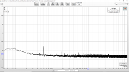
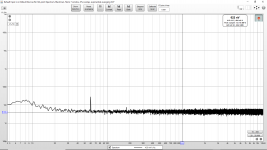
- DVDD
- DVDD (different timebase)
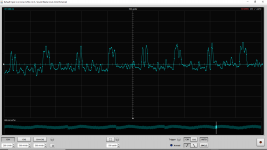
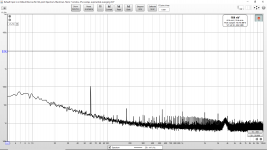
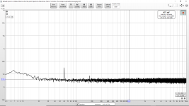
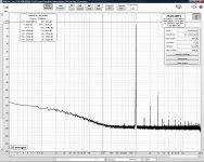
- DVCC
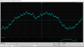
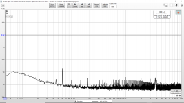
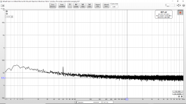
- VCCA
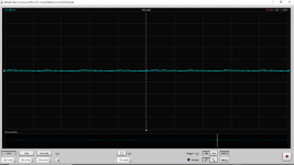
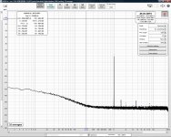
- AVCC_R (5uV scale)
Initial Conclusions:
The large 85Hz noise component is much stronger on the DVCC pin (not DVDD). This may provide information on the source of that LF noise component. This might be useful information for further surpressing that noise component. Question: Would a lower impedance on DVCC further lower this noise component on DVCC? (Lower impedance either from an active or passive source. Again just looking for information at this point.)
The other large (HF) component of DVDD noise is largely not seen on VCCA (or AVCC_R for that matter). (This may also be useful information on deciding on the suitable modifications and types of circuits/supplies.)
DVDD bypassing changes have a very small impact on the observed DVDD noise.
In addition DVDD bypassing changes have almost no impact on the observed noise on other pins (importantly VCCA and AVCC_R).
These results are not surprising. However it was considered worthwhile to at least measure the DVCC noise which was previously largely unknown (to me).The other large (HF) component of DVDD noise is largely not seen on VCCA (or AVCC_R for that matter). (This may also be useful information on deciding on the suitable modifications and types of circuits/supplies.)
DVDD bypassing changes have a very small impact on the observed DVDD noise.
In addition DVDD bypassing changes have almost no impact on the observed noise on other pins (importantly VCCA and AVCC_R).
As per the previous measurements the soundcard bandwidth is clearly limited and can not observe RF. That said the ESS demo board schematic has only the same single 1uF ceramic on all five pins, so the present ceramic plus 22uF tantalum on each pin (stock) does not seem abnormal or obviously deficient. Of course we don't know much about the 1206 ceramic capacitors that are installed (stock). Also the 100kHz to 300kHz performance of the OS-CON solid polymer capacitors is a pretty decent addition to the stock ceramic and 22uF tantalum.
A question for those with more experience and knowledge of the ESS demo board: Does the ESS recommendations/literature or demo board bypassing indicate significant concern for RF? [Just one 1uF and the same on all pins seems rather basic or even like a default choice.] Hopefully some useful clues from ESS?
Edit: I find it a little odd that the ESS ES9038Q2M schematic (that I found) has only 1uF while the their recommendation appears to be 4.7uF ±20%, X5R 6.3V 0402.
If anyone has higher bandwidth (RF?) measurements please post.
Attachments
-
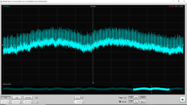 100uF Xicon DVDD All Battery Powered Optical Locked Time Base.png98.6 KB · Views: 368
 -
 100uF Xicon DVDD All Battery Powered Optical Locked.png92.2 KB · Views: 376
 -
 100uF Xicon DVCC All Battery Powered Optical Locked Time Base.png91.8 KB · Views: 369
 -
 100uF Xicon VCCA All Battery Powered Optical Locked Time Base.png47.1 KB · Views: 351
 -
 100uF Xicon AVCC_R 5uV All Battery Powered Optical Locked Time Base.png89.2 KB · Views: 355
Last edited:
IMHO only, the ESS evaluation boards are designed to show its easy to get very good measured AP metrics at minimal cost. Lots of bells and whistles built into one chip helps cut consumer product manufacturing costs, and helps sell more dac chips.
Making a dac that measures very well and sounds exceptionally good too is more complicated. Designers are on their own, no eval board tailored for that tiny market segment.
Making a dac that measures very well and sounds exceptionally good too is more complicated. Designers are on their own, no eval board tailored for that tiny market segment.
I see. I made the mistake of assuming that ESS was aiming at demonstrating very high performance and sound quality, not (just) mass market measured metrics.
Last edited:
Can someone please explain to me the relative ranking (in terms of performance when used with the ES9038Q2M board in this thread) of the following:
I assume the XMOS is best. How much better is it than the next best? Vastly? A little bit?
Are there others (that are currently available) that I should consider? WM? BB/Ti?
- XMOS U208
- CS8416
- SA9023A
- CM6631A
I assume the XMOS is best. How much better is it than the next best? Vastly? A little bit?
Are there others (that are currently available) that I should consider? WM? BB/Ti?
It isn't just the chip, its the implementation. What I would probably consider the best USB board: I2SoverUSB - I2S over USB Audio ....Although the new Chinese USB boards with AS318 clocks sound a bit better in terms of audible jitter effects, but they need modding to power from a clean 5v supply instead of using USB power, or they don't sound so good. Same trick works for a real Amanero USB board (Chinese clones aren't so good), but clocks are not the best (although they can be fine with external clocking).
A good SPDIF Receiver/ASRC is SRC4392 (and a lot of good implementation info in the datasheet). I like AK4137 better, but they are getting hard to come by due to the AKM factory fire.
Haven't tried CS8416 which is a SPDIF receiver only, no ASRC.
If not designing in a FIFO to sync SPDIF with the dac clock, I would opt for good ASRC using the dac clock as the reference. Since the dac clock is 100MHz and you would probably need 1/4 of that for an ASRC reference, I would probably try using ICS542 to do the dividing.
Last edited:
Too late to edit last post. Should have mentioned AK4137 is an ASRC only. The SPDIF receiver AKM makes is AK4118. SRC4392 is a good part that can do both functions, but unlike AK4137, SRC4392 can't convert PCM to DSD.
So if I am understanding this correctly the AK4137 can take in PCM (such as from a CD played in a DVD player via SPDIF) and output DSD? (Thus avoiding the cost of a computer and software to do it?)
And I imagine the quality limitations are at least one if not two orders of magnitude below that of the output stage on this board?
And of course they are in scalper territory right now.
And I imagine the quality limitations are at least one if not two orders of magnitude below that of the output stage on this board?
And of course they are in scalper territory right now.
It takes two AK4137 to do it right, that's because they are only good at producing DSD256 if they don't have to do upsampling at the same time. So, the first AK4137 does the upsampling, and the second one does the DSD conversion.
If everything is synchronously clocked, USB board, AK4137s, and dac chip, that is ideal. It means the polyphase upsampling filters should hopefully always be using the same coefficients (that is, so long as we can help stabilize the PLL with clean power and a low-jitter reference clock).
Efforts to do most of those things reasonably well can be seen in the Beaglebone DSD thread. Schematic is attached to the first post. Can it be done better? Sure. I can see opportunities to tweak the design up a notch or two, but it would raise cost and complexity.
Last edited:
So the pieces are starting to be put together for testing. (Just inside a shielded tin without the DAC.)
The prototype is inside a shielding tin. The LNA is inside a second shielding tin. The two shielding tins are isolated. The “reference” in this case is just a regular ADJ bypassed LM317 followed by a capacitance multiplier as described in my prior post where I recreated the capacitance multiplier results publish in the EDN article.
The enclosed results (in order) are:
The “filter” here is 200 Ohms and regular ESR 100uF 25V Xicon. (It is like the post 3003 op amp buffer/filter but using NE5532 and different values and types for the capacitors and resistors.)
Could someone help me out with a back of the envelope calculation of the output impedance of the NE5532 used as a unity gain buffer/follower? Or LT Spice if you have it.
The fake NE5532 data is included so that you can be warned about what to expect when you order op amps from low cost non-authorized sources.
The prototype is inside a shielding tin. The LNA is inside a second shielding tin. The two shielding tins are isolated. The “reference” in this case is just a regular ADJ bypassed LM317 followed by a capacitance multiplier as described in my prior post where I recreated the capacitance multiplier results publish in the EDN article.
The enclosed results (in order) are:
- Noise of 60 dB LNA shorted to prototype.
- Noise at the capacitance multiplier output using the cheapest 680uF 16V (ChongX) capacitor.
- Noise at the capacitance multiplier output a 2200uF 16V Low ESR capacitor.
- Noise at the output of the op-amp filter/buffer using a fake NE5532.
- Noise at the output of the op-amp filter/buffer using a genuine Ti NE5532.
The “filter” here is 200 Ohms and regular ESR 100uF 25V Xicon. (It is like the post 3003 op amp buffer/filter but using NE5532 and different values and types for the capacitors and resistors.)
Could someone help me out with a back of the envelope calculation of the output impedance of the NE5532 used as a unity gain buffer/follower? Or LT Spice if you have it.
The fake NE5532 data is included so that you can be warned about what to expect when you order op amps from low cost non-authorized sources.
Attachments
-
 Output of Op Amp Buffer Genuine Ti NE5532 200Ohm 100uF Input Filter.png75.3 KB · Views: 140
 -
 Output of Op Amp Buffer Fake NE5532 200Ohm 100uF Input Filter.png72.4 KB · Views: 155
 -
 Output of Cap Mult After LM317 Low ESR Cap.png79.1 KB · Views: 148
 -
 Output of Cap Mult After LM317 Regular ESR Caps.png80.7 KB · Views: 171
 -
 60 dB LNA Shorted on DUT.png120.6 KB · Views: 155
Last edited:
Continued from the last post here is a comparison of different op-amps tested in the same op-amp filter/buffer:
- Fake NE5532
- Genuine Ti NE5532
- Genuine ST LM833N
- Genuine Xinluda XD833
- Genuine JRC 5532DD
- Genuine JRC 4580D
- Genuine JRC 4562D
- Genuine National LM4562AD
Attachments
-
 Output of Op Amp Buffer National LM4562NA 200Ohm 100uF Input Filter.png73.9 KB · Views: 162
 -
 Output of Op Amp Buffer JRC 4562D 200Ohm 100uF Input Filter.png71.3 KB · Views: 159
 -
 Output of Op Amp Buffer JRC 4580D 200Ohm 100uF Input Filter.png71 KB · Views: 154
 -
 Output of Op Amp Buffer JRC 5532DD 200Ohm 100uF Input Filter.png72.5 KB · Views: 175
 -
 Output of Op Amp Buffer Xinluda XD833 200Ohm 100uF Input Filter.png72.9 KB · Views: 144
 -
 Output of Op Amp Buffer ST LM833N 200Ohm 100uF Input Filter.png70.9 KB · Views: 164
 -
 Output of Op Amp Buffer Genuine Ti NE5532 200Ohm 100uF Input Filter.png75.3 KB · Views: 157
 -
 Output of Op Amp Buffer Fake NE5532 200Ohm 100uF Input Filter.png72.4 KB · Views: 164
I was able to get the ancient Vista machine with the Creative Professional/E-MU 1820 running again. Now I have SPDIF working with 24 bits with ASIO drivers for REW. (With the SB0490 I only had SPDIF working with 16 bits since REW using Java drivers in Windows is limited to 16 bits. And the SPDIF output on the SB0490 does not even show up as an option in ASIO4ALL.)
As a result I was able to run J-TEST on the ES9038Q2M board in this thread. So E-MU 1820 SPDIF to ES9038Q2M via optical. (Running on batteries with low ESR capacitors but otherwise not modified. Using the original voltage output stage but with LM4562 op amp.)
Please take a look. Does it look right? (I have never run J-TEST before.) If I am interpreting the results correctly does this mean the jitter is very good?
Attachments

I used the J-test option in the REW generator.
I tried to copy post 22 from the REW J-test on AK4490 shown here: https://www.diyaudio.com/forums/digital-line-level/365976-modular-ak4490-dac-3.html#post6506619
Does this agree with the jitter measurements others have done on this ES9038Q2M board?
I tried to copy post 22 from the REW J-test on AK4490 shown here: https://www.diyaudio.com/forums/digital-line-level/365976-modular-ak4490-dac-3.html#post6506619
Does this agree with the jitter measurements others have done on this ES9038Q2M board?
Last edited:
If I am interpreting the results correctly does this mean the jitter is very good?
You have some of the sidebands visible at -145dB but otherwise the jitter looks to be ok.
Ok. Great. Considering the poor performance of the stock voltage mode output stage on my ES9038Q2M board I am concluding that the jitter is perfectly fine for my needs. [In other words this level of jitter performance is the least of my problems relative to the stock output stage.] Perhaps the IV output stage should be next.
Last edited:
After switching from the SB0490 to the E-MU 1820 I can better measure this board before further changes.
Based upon the attached I am concluding that I need to replace the output stage before anything else.
Markw4, can you confirm that these very high 2nd and 3rd harmonic levels are due to the voltage mode output stage? Do these measured levels match the signature of that problem? If it is that bad I think I need to fix that before proceeding with anything else.
Attached, in order:
- -60 dBFS
- -10 dBFS
- -6 dBFS
- -3 dBFS
- 0 dBFS
Attachments
-
 ES9038Q2M 0 dBFS Measured by E-MU 1820 to MIC A dB.jpg235.6 KB · Views: 153
 -
 ES9038Q2M -3 dBFS Measured by E-MU 1820 to 1 MIC A dB.jpg235.3 KB · Views: 318
 -
 ES9038Q2M -6 dBFS Measured by E-MU 1820 to MIC A dB.jpg233.4 KB · Views: 302
 -
 ES9038Q2M -10 dBFS Measured by E-MU 1820 to MIC A dB.jpg233.7 KB · Views: 304
 -
 ES9038Q2M -60 dBFS Measured by E-MU 1820 to MIC A dB.jpg232 KB · Views: 330
J-test maybe too good to be true. Can you try optical, or substitute the SPDIF cable with a long, cheap audio cable, not 75-ohm? In other words, see if you can make jitter much worse and see how the spectrum changes. Does that make sense?
Given that ESS dac chips have ASRC designed to attenuate jitter, your results probably shouldn't look any better than those for similar dac designs published at ASR, Stereophile, etc.
Also, there is what looks to be a 24-bit jitter wave file in one of the first few posts in the thread at: Jitter Test Signal (J-test Signal) with MATLAB
If using ASIO, you could play it through foobar2000 (after installing its ASIO component). Digital volume control should be all the way up. The sound blaster card should not be assigned as Windows default sound device, nor as the default communication device. You may be able to view the spectrum in REW if it allows you to set separate input and output audio devices. Otherwise, REW may own the sound blaster ASIO output device so foobar2000 might not be able to use it.
In other words, I suggest doing some of what I would call 'sanity' checks.
EDIT: High 2nd and 3rd HD are normal for voltage mode.
EDIT 2: Jitter as measured by J-test is not good for measuring close-in phase noise. Its level is only roughly suggested by the width at the root of J-test signal FFT peak. Many people find that phase noise does affect sound quality though, and there is some simulation results in another thread suggesting it can cause dynamic masking of music spectral components close in frequency to each other. Actually in SD dacs such as ESS, jitter and phase noise can have much more complex effects that are described in some books and papers on SD dac theory and design. Bottom line for me, a good and credible J-Test result is good but it doesn't mean there aren't audible jitter/phase-noise problems not shown by J-Test.
Last edited:
Ok. I'll try to go back to the jitter again later to confirm. These measurements were done with an optical SPDIF connection. The E-MU 1820 external dock has only optical SPDIF but I looked and found coax SPDIF connectors on the PCI card. I could try that. I had forgotten those connectors on the back of the computer.
By the way it is not the SB0490 for the measurements done today. It is the E-MU/Creative Professional 1820. (Quite a step up from the SB0490 that I was using.)
Edit: One data point I found from an earlier variant of this board design is: Measurements Of Generic ES9038Q2M DAC Board | Audio Science Review (ASR) Forum
Last edited:
@kozard
There are a lot of similarities compared to my measurements. You can find them here:
ES9038Q2M Board
You can also find measurements using a current mode output.
I just wonder where the low frequency noise (below 300 Hz) in your measurements comes from. Is it from your sound card?
There are a lot of similarities compared to my measurements. You can find them here:
ES9038Q2M Board
You can also find measurements using a current mode output.
I just wonder where the low frequency noise (below 300 Hz) in your measurements comes from. Is it from your sound card?
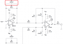
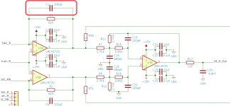
I was looking at a number of I/V stage schematics and I noticed that one I/V schematic for the PCM1794 used 820Ohms (R1) and 2200pF (C1) while one ES9038Q2M I/V schematic used 820Ohms (R1) and 330pF (C1).
I know the PCM1794 is 192kHz and ES9038Q2M is 384kHz but with the same resistor in the I/V stage the capacitor ratio is closer to 10x than 2x. (See attached, first PCM1794 with 820Ohms and 2200pF, second ES9038Q2M with 820Ohms and 330pF.)
I am curious why/how the capacitor values are so different?
I know the PCM1794 is 192kHz and ES9038Q2M is 384kHz but with the same resistor in the I/V stage the capacitor ratio is closer to 10x than 2x. (See attached, first PCM1794 with 820Ohms and 2200pF, second ES9038Q2M with 820Ohms and 330pF.)
I am curious why/how the capacitor values are so different?
Attachments
- Home
- Source & Line
- Digital Line Level
- ES9038Q2M Board