The gain board with limiter and low noise supplies sums up to an unpleasant size.
Already the components which I really want to have as pin-through-hole devices consume the entire board.
Have a look to the attached picture.
The resistors, diodes and caps on the right hand side, but displayed outside the
board won't fit in pin-through-hole-style, but could be solved as SMD.
As 0805 SMD types I guess that they will fit on the back side.
Who would be in trouble with 0805 SMD components on the gain board?
Astx: As I understood, you would dislike the SMD, but you intend to go for your own discrete input stage.
So the gain board would not give you headache - right?
Attachments

...
Astx: As I understood, you would dislike the SMD, but you intend to go for your own discrete input stage.
So the gain board would not give you headache - right?
You are right!

Very nice work!
Not me (and presumably not anyone with a temperature controlled soldering iron and appropriate magnification); make them 0603 if you like. Just watch out for thermal tracking errors.Who would be in trouble with 0805 SMD components on the gain board?
Ok, I see 0805 seems to be acceptable for most.
Personally in my DIY assortment, I enjoy to use 0805, but do not stock 0603 or smaller...
twest820:
Do you have particular concerns regarding thermal tracking with the circuitry of posting #86?
...I mean we are heading for audio not for a thermocouple gain stage.
Basically I think the drift of the power stage will dominate over any reasonable OP amp implementation of the gain stage. So far I did not intend to superimpose a global integrating loop using the gain stage for DC-perfection, which of course also would be possible.
Or am I missing something?
Good 0805 resistors (Susumu RR or RG) typically have a 25 ppm TCR. So a one degree temperature rise from self heating yields a gain shift of around -92dB for a typical op amp stage. This tracks the signal to the extent allowed by the thermal time constant of the resistor and traces. More heating yields correspondingly more gain drift. Depending on device performance, signal level, feedback impedance chosen, layout, and program material the result may be a lift of the IMD floor above the noise floor or the op amps' internal limit.
At a glance I'd expect the circuit of post 86 to be OK for consumer input levels. For pro audio levels with good gain structure it'd likely be bypassed. It's that middle ground between the approximately -10dBV consumer audio line level and the 16dBu of optimized pro audio which gets interesting. Depending on what you wish to support the 4 dBu nominal pro audio line level might be an interesting case to consider. (Some of us would roll resistors as needed but not everyone has that level of know how.)
At a glance I'd expect the circuit of post 86 to be OK for consumer input levels. For pro audio levels with good gain structure it'd likely be bypassed. It's that middle ground between the approximately -10dBV consumer audio line level and the 16dBu of optimized pro audio which gets interesting. Depending on what you wish to support the 4 dBu nominal pro audio line level might be an interesting case to consider. (Some of us would roll resistors as needed but not everyone has that level of know how.)
Glad to see that you getting the same numbers like I do....gain shift of around -92dB
Well...
- THD of the LiteAmp approaches -100db at 1W levels.
- THD+N of the LiteAmp is between -80db...-90db.
- IMD slightly worse.
- Last but not least CMRR is usually limited by our personal matching accuracy of resistors, means most people won't reach much more than 60dB.
That's where I see the bottlenecks which are pretty likely to dominate over the thermal tracking.
No doubt, preferred gain depends on the entire chain and personal taste.At a glance I'd expect the circuit of post 86 to be OK for consumer input levels. ....
..wish to support the 4 dBu nominal pro audio line level...
Some of us would roll resistors as needed but not everyone has that level of know how.
Thanks for pointing to this topic. I will add a comment regarding Rgain, which allows to adjust gain by a single resistor without needing to rematch any other resistors.
The gain stage with values like in posting #86 has a gain of 5.3.
Combined with the LiteAmp main board an input level of 0dBu will lead to approx 100W into 4R.
Can you tell which pair or pairs would determine CMRR? I don't immediately see any, except at the zener current limiters. But these resistors only influence the opamp power supply, and the opamp has it's own CMRR.
Kind regards,
Marc
Kind regards,
Marc
...with ideal OP amps... Kirchhoff tells us that two ratios must equal:
R119/R117 = R120/118
Which you can translate into two matches:
R118 = R117
&
R119 = R120
These two matches ensure that the ratios are OK and additionally ensure that the drive impedances of both inverting OP amp inputs are identical ...and could be designed to fit the expected drive impedances at the inputs of the instrumentation amplifier.
However when you use OP amps with FET inputs, then some k-Ohms imbalance of the drive impedances would be no real show stopper. At least not within audio bandwidth.
Oh dear, I was in another world. CMRR of coarse is influenced by opamp inputs, I was considering PSRR, which is a different beast. Anyway, even a decent modern bipolar input opamp would not suffer too much in this respect (CMRR and input bias).
There seems to be an assumption parts selection and layout will hold resistor heating substantially below 1C. The point is that's worth verifying if performance is a critical parameter. Keeping 0805s below 250mC Trise tends to want some design effort but that's what's required if one wants to avoid lift of a -90 to -100dB IMD floor.Well...
Looks like you're planning to use film caps for AC blocking so, yeah, impedance matching for CMRR will be dominated by resistor tolerances rather than cap ESRs or trace layout. Agree 60dB is optimistic considering chassis temperature elevation and drift over load life---to guarantee it something like 0.01% 2ppm Susumu RGs are needed as a starting point---so I tend to see it as a question of desired common mode handling. If you figure a 10 or 20uV noise floor in the circuit and 40dB CMRR that'll do for a mV or two of offset. Much beyond that and a difference amplifier's easier and cheaper.
Speaking of common mode offsets it's easy to end up with grounding error terms 70 or 80dB down. Post 86 doesn't obviously show remote ground sense so I'm not sure what you're thinking for handling the board to board transition and ground offsets from the power stage's current pull. It's worth fussing over as well.
Depends upon what one considers acceptable. Ground offsets between audio devices or boards within a chassis tend to be microvolts or a few millivolts, with various less friendly cases running to a few hundred millivolts. I generally look at a one volt offset as a worst case. With the 35 to 50dB CMRR of typical discrete difference amplifier implementations that yields around 10mV error worst case. That's comparable to the offset a modern BJT op amp with uncompensated input bias like the OPA1632 generates in a 10k resistor.even a decent modern bipolar input opamp would not suffer too much in this respect (CMRR and input bias)
Compensated BJT op amps with nA bias reduce offsets to a few hundred uV, resulting in offsets often competitive with the input voltage offsets of FET input op amps. In principle, a more critical parameter is the input offset current. That's usually around 10nA in compensated designs, implying a nominal bias shift of around 100uV through a 10k feedback network as the operating point changes. In practice it doesn't seem to be an issue, suggesting bias changes are sufficiently linear to be at or under the few tens of uV typical of audio circuit noise floors or common mode error residuals in balanced circuits.
The frontend impedances in post 86 are low enough a well chosen BJT op amp would be lower noise than a FET part, though I'd be surprised if the optimization was meaningful in the overall circuit (would have to sim it to see). From a noise standpoint the 100k feedback on the backend wants a FET part. If one wants to get a little more out of the circuit I'd suggest the OPA1652 and OPA1654, their main advantage being the extra 5 to 7dB loop gain over the OPA2134 and TL074 (1652's cheaper than the 2134, too).
No doubt. In terms of CMRR and long term drifts any integrated difference amp will perform much better. Soundwise I have no opinion on integrated difference amps, never listened to them.
Do you recommend to use them? Do you have a preferred type?
My reason for the solution with OPA2134 is that I want to keep the costs and amount of special components low. (However I still could change the design and extend the set of key components.. ..what's your advice?)
OPA2134 is a decent quality type, which is easily available. The design will still work with an TL072, TL082, or even bipolar NE5532 when some DIYers cannot get high quality OP amps.
True, OPA1652 is likely to be a good candidate instead of the OPA2134, especially noise figures of OPA1652 are great for a FET type.
However I am not sure that it will make much difference with the noisy IRS2092 behind... 🙄
OPA1654 instead of TL074 also is likely to work fine - but it would be a waste of pearls, the entire TL074 circuitry is just the control mechanism for the limiter and is not influencing the signal, except at overdrive levels via the Vactrol.
GND:
No remote GND sensing intended.
In class D I am experiencing best signal integrity with closed GND planes and controlling the current densities and resulting GND errors + noise by the positions of the devices.
This positioning is particular crucial with the switching stage, where the LiteAmp has to deal with currents up to 30 amperes and fast di/dt in the category of 500A/us...1000A/us and having small signal circutries close by.
At that end of the PCB where the gain board is coupled to the main board no high currents are expected.
The concept extends the GND plane towards the gain board via a grid of 12 pins. Each pin has approx. 1.8m Ohms including soldering.
A grid of 12 paralleled pins should results in 150 micro Ohms and low inductance.
Loaded with some 20mA...30mA I am ending up below 5 microvolts GND error. With input signals of 1V this is -106db, allowing also higher gain settings and smaller input signals without catastrophies.
Even at this end of the PCB I am not convinced that the transient noise from the switching stage would be less than the 5uV GND error caused by the gain board current draw....
Do these GND considerations contradict with your switch mode power experiences?
I'd let the TL074 be but consider an OPA1652. Bruno Putzeys' derivation one needs around 18MHz GBP in a Miller compensated linear amp for reasonably transparent audio agrees with my personal ABX results. It's not a big difference in my experience but might offer a little on the top end. Since 0805 is fine the 1652 being SOIC is no problem. The distributors I use charge less for a 1652 than a 2134.However I still could change the design and extend the set of key components.. ..what's your advice?
If someone needs or wants to roll to a 2134 I'd expect it to be no problem since decreasing loop gain rarely causes stability issues. It is one more thing to check, though.
The most interesting space is typically 10 to 20kHz rather than at the resistive limit. Error terms are larger due to inductance and corrections tend to be less due to reduced loop gain. You're sufficiently far ahead of me in figuring out how to take advantage of IRF's error amplifier I think the best I can do is to refer you back to a search of Eva's posts where she talks about minimizing inductance to keep switching transients localized and avoiding carrier feedback to the linear components in the signal chain before the comparator.Do these GND considerations contradict with your switch mode power experiences?
In the composite linear amps I've collaborated on there was no problem measuring degradations from the ground bounce across ~3nH. Errors were about 90dB down, which is within scope for the LiteAmp.
If high CMRR is needed difference amplifiers are substantially smaller and cheaper than signal transformers. Whether or not it's needed is a maybe. If you work your grounding and class I and II appliance setup the answer is it's not. If you'd prefer to throw an extra euro or two's worth of hardware at the problem and not sweat the system grounding the answer is probably yes.Do you recommend to use them? Do you have a preferred type?
Default circuit design in pro audio is any ground transition has a TL072 based difference amplifier on each side, some kind of remote sense/pseduodifferential connection, 0805 10k feedback networks, and a pair of 220pFs for lowpass. Figure 1% resistors and 5% caps, meaning CMRR is limited by cap matching across most of the audio band and not anything special. One way of looking at this is entry level balanced is good enough for the day in, day out business of schlepping audio through pedal chains, ADCs, DACs, mixing desks, and instrument amps. Taken naively this suggests it should be good enough for home audio too.
But. There are mitigating factors in pro audio which don't apply in home audio. Live sound and recording components are typically low to no power and often many cables are connected in parallel between devices. So ground bounce is small to start with and shorted by lower impedances than found in home audio. Also, there's usually an iso box (signal trafo) handy to grab if a hum problem comes up. In home audio it's more like a couple unbalanced to balanced cables from a USB DAC to a power amp. More bounce, higher impedance, no iso option. At least there's some approximation of a remote sense if the cables are right.
The reason THAT and TI make difference amplifiers suitable for audio use is there's enough demand from the higher end of the pro audio market to keep their line driver and receiver product lines afloat---in the better gear there's an informal convention it should handle something like 100mV AC common mode with acceptable results. Throw a few dB margin on that for the home audio case and you know where I got the 1V stress test case I mentioned in my previous post. How often is the 30 or 40dB CMRR of basic balanced not enough? I don't know. I've spent more time measuring ground offsets between consumer devices than most folks and used some extremely nice (expensive) gear to do it. I would guess a comprehensive ABX testing campaign would show subjective improvement in something like 1 to 5% of cases.
I do know I've never built a power amp without balanced input and probably never will. The most recent design is a bit of a premium one so it uses THAT 1200s. For low cost look at a TL074 in front of a THAT 1290 to make a couple instrumentation amps. (Analog has a few interesting parts too.)
My referencing of GND errors towards the line level input was misleading. Sorry for this.
The line level input is routed fully differential from the main board to the gain board (of course with reasonably small enclosed loop area).
Only the signal from gain board towards the power amp is asymmetric, which I am not afraid of, because signals are large. Voltage gain of the power amp on the main board is less than factor 5.
Thanks for pointing to the THAT1200. Bootstrapping an input center tap in order to achieve high common mode input impedances over a wide bandwidth. Nice.
Personally I like the INA types from TI. Their ref pins can be routed the relevant GND point and TI gives access to the nodes which you need for custom gain setting.
However the pricing at digikey and mouser is a clear no go for this project
I definitely intend to keep the dual OP amp as a DIL provision in the PCB, so everybody can experiment with his favorites.
For playing with OP amps in SOIC package I will use adaptors.
Besides OPA1652, also AD8620 and AD8066 are in my focus. If they need to be tamed in terms of frequency compensation, it can be integrated on the adaptor.
From construction I expect the GND grid between main board and gain board to be in the region of 1nH or even less.
The line level input is routed fully differential from the main board to the gain board (of course with reasonably small enclosed loop area).
Only the signal from gain board towards the power amp is asymmetric, which I am not afraid of, because signals are large. Voltage gain of the power amp on the main board is less than factor 5.
Good point. Means the solution of posting #86 is already better than average and can be stripped to normal level by using a TL072...Default circuit design in pro audio is any ground transition has a TL072 based difference amplifier on each side, some kind of remote sense/pseduodifferential connection .... Taken naively this suggests it should be good enough for home audio too.
Thanks for pointing to the THAT1200. Bootstrapping an input center tap in order to achieve high common mode input impedances over a wide bandwidth. Nice.
Personally I like the INA types from TI. Their ref pins can be routed the relevant GND point and TI gives access to the nodes which you need for custom gain setting.
However the pricing at digikey and mouser is a clear no go for this project
OPA1652 in SOIC is no issue - but the other way round.Since 0805 is fine the 1652 being SOIC is no problem.
I definitely intend to keep the dual OP amp as a DIL provision in the PCB, so everybody can experiment with his favorites.
For playing with OP amps in SOIC package I will use adaptors.
Besides OPA1652, also AD8620 and AD8066 are in my focus. If they need to be tamed in terms of frequency compensation, it can be integrated on the adaptor.
10 to 20kHz is sort of DC in switch mode power environment, I definitely prefer to place a low inductive grid of 12 pins for the GND connection rather than a single connection with remote GND sensing.The most interesting space is typically 10 to 20kHz rather than at the resistive limit.
Come on.. 🙄 Eva only published some of her early learnings and experiences. Her later growth is hidden.... refer you back to a search of Eva's posts where she talks about minimizing inductance to keep switching transients localized ...
Thanks, that's definitely a valuable input.In the composite linear amps I've collaborated on there was no problem measuring degradations from the ground bounce across ~3nH. Errors were about 90dB down, which is within scope for the LiteAmp.
From construction I expect the GND grid between main board and gain board to be in the region of 1nH or even less.
Come on.. Eva only published some of her early learnings and experiences. Her later growth is hidden.
😀 True that.
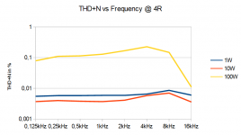
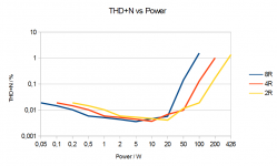
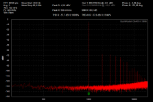
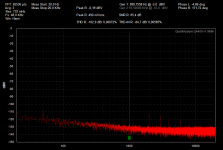
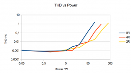
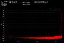
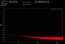
Performance of Main Board
...measurements done with +/-43V rails:
Idle noise is 75uVrms. Relative to 100W @ 4R this means -111db.
Attached pictures:
+ THD vs Power
+ Spectrum 1W @ 4R
+ Spectrum 10W @ 4R
+ Spectrum 100W @ 4R
+ THD+N vs Power
+ THD+N vs Frequency
+ 426W @ 2R
...measurements done with +/-43V rails:
Idle noise is 75uVrms. Relative to 100W @ 4R this means -111db.
Attached pictures:
+ THD vs Power
+ Spectrum 1W @ 4R
+ Spectrum 10W @ 4R
+ Spectrum 100W @ 4R
+ THD+N vs Power
+ THD+N vs Frequency
+ 426W @ 2R
Attachments


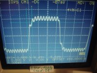
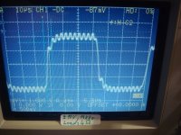
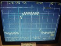
Performance of Main Board ...continued...
+ IMD 1W @ 4R
+ IMD 10W @ 4R
+ IMD 100W @ 4R
+ Rectangle, +/-10V, 14kHz, 8R
+ Rectangle, +/-10V, 14kHz, 4R
+ Rectangle, +/-10V, 14kHz, 2R
+ Complex signal handling, +/-20V triangle(1kHz) & +/-5V rectangle (8kHz), 4R
+ IMD 1W @ 4R
+ IMD 10W @ 4R
+ IMD 100W @ 4R
+ Rectangle, +/-10V, 14kHz, 8R
+ Rectangle, +/-10V, 14kHz, 4R
+ Rectangle, +/-10V, 14kHz, 2R
+ Complex signal handling, +/-20V triangle(1kHz) & +/-5V rectangle (8kHz), 4R
Attachments


- Home
- Amplifiers
- Class D
- SystemD LiteAmp