Due to the twice as large heat transfer area in the latter case, thermal resistance of the whole setup is also higher by the same factor.
I hope this helps.
Regards,
Braca
Should have read "lower". Sorry about the mistake.
Regards
Braca--how are you accounting for the major differences in thermal conductivity between the copper block with a thin epoxy layer (to the back) and the thick epoxy layer to the front?
Given these paths can be modeled (in effect) in parallel, and the epoxy-only path is much higher resistance, the total resistance is going to be almost completely dominated by the lower resistance path.
It's never a question of whether the copper blocks will help, but a much bigger question of how much. Given the machining necessary, it seems to me making a circuit that parallels multiple chips would cost less and have much, much higher power capacity.
So, yes, the 2 K/W will drop a little with the copper block, (1.95?) but nowhere near as much as paralleling 2 chips (which, in effect, may give you ~1.1 equivalent).
Braca--how are you accounting for the major differences in thermal conductivity between the copper block with a thin epoxy layer (to the back) and the thick epoxy layer to the front?
Given these paths can be modeled (in effect) in parallel, and the epoxy-only path is much higher resistance, the total resistance is going to be almost completely dominated by the lower resistance path.
It's never a question of whether the copper blocks will help, but a much bigger question of how much. Given the machining necessary, it seems to me making a circuit that parallels multiple chips would cost less and have much, much higher power capacity.
So, yes, the 2 K/W will drop a little with the copper block, (1.95?) but nowhere near as much as paralleling 2 chips (which, in effect, may give you ~1.1 equivalent).
Thank you for your comment, Derfnofred.
Assuming that the internal copper plate of the 3886 extends past the mounting hole, we have the same thermal conductiivity, i.e. the value in the rearward direction, at the face of upper part of the casing's mounting section, which accounts for about 35% of the face area. While it is true that the facewards thermal conductivity over the rest of the face area will be higher (by a factor of 3 on the average, maybe) than the rearwards one, there is also a larger heat transfer surface in the cooling block case (don't forget the 11 electrical pins above the internal copper block, which improve the faceward heat conduction), such that my estimate may still hold. As a matter of fact, I calculated the total thermal resistance of LM3886 in the block to be about 1.2 K/W.
Considering the machining, in a country with an average salary of about 300 US$, and with electronic components due to duties and taxes being more expensive than in the West, it is not a bad deal.
Regards,
Braca
Hi, Braca,
Perhaps the mounting tab will be able to soak up a lot more heat, and as you say, we'll get much better heat transfer. The proof is indeed in the eating of the pudding. 🙂
Copper is expensive, no matter the origin. You might make an argument for aluminum's cost effectiveness if indeed there is a material advantage in heat transfer.
Either way, it's all speculation until we see some measurements.
Yes, I thought I'd say it again since the OP seemed to have missed it and appeared to think that you can always get the die cold by using a big enough heatsink. Which is not true of course - there's alway the T-difference between die and heatsink ... 😉
So for 100W and 2K/W that difference is 200 degrees when dissipating 100W. To get the die below 165 degrees the heatsink must be below -35 no matter how big or fancy ....
No worries. This does indeed appear to be one of those cases where over-communication is called for. I appreciate you chiming in.
~Tom
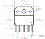
why everyone forgets front side part where screw goes? could this be place of lower thermal resistance?
edit: isnt die to case measured only on back side?
This entire discussion has included the thermal resistance from the die to the front of the package as that's what you claim makes your clamping block work. As I, and others, have described over and over in this thread, the thermal resistance through the top of the package is significantly greater than the thermal resistance through the back of the package. This is obvious if you look at the image I posted a few pages back. Here it is again:

Notice how the plastic on the top of the die is about four times thicker than the plastic between the DAP and the back of the package? How do you think this impacts the thermal resistance through the front of the package. Also, the contact area on the front of the package is much smaller than that of the back of the package. How do you think this affects the thermal resistance out the front of the package? I'm very curious about your reasoning here. What are your thoughts?
You may want to re-read these posts (I've linked them to make it easier for you):
Post #240.
Post #227.
I also suggest reading the very informative posts by jneutron.
We all understand what you are trying to do and how you claim your clamp works. We all agree that the clamp won't provide any meaningful benefit and have explained why several times. It's unfortunate that you won't listen, but none of us who are trying to teach you have the ability to change that.
Look at the bright side: At least you got to have some fun with the milling machine...
~Tom
Last edited:
No worries. This does indeed appear to be one of those cases where over-communication is called for. I appreciate you chiming in.
~Tom
With all due respect, IMHO this is not the matter of a big heat sink, but rather the one of the heat transfer area at the chip package. Of course, dissipating 100W does call for a larger secondary heat sink in order to keep the temperature of the whole assembly sufficiently low, but it is a routine matter.
Regards,
Braca
Well... I'm looking forward to seeing the data.
~Tom
Well, I happen to know the man (Macola) who did the experiment very well, as I'm responsible for directing him to electronics at the age of 10. I was not present at this particular test, but I know that he uses this sort of cooling on a routine basis in his industrial electronics projects that involve powers in the several hundred kW range.
He is also a man of impecable integrity, but I'm nevertheless ask him to send me some numbers, although the test he performed was one of endurance, i.e. the LM's were forced to dissipate 100W per IC for hours, and none of them failed.
Regards,
Braca
I'm trying to recall when this whole idea started (power semi maker selling versions with insulated tab/case as well as the usual chip directly mounted on externally exposed metal). Were these (then) National audio chips the first?
I recall when many power devices used mica (or perhaps other material) insulators between the part body and the heat sink. Has this gone out of favor?
What I especially want to know is how does the insulated-die thermal spec compare with the old-fashioned way of electrically insulating from a heat sink Is there a discussion/comparison of this somewhere?
Wait a minute - this board has all these smilies, but not one eating popcorn? I'm wanting to sit back and watch what happens at power-up of a looks-fine-but-perhaps-too-thin layer of insulation on one of these things.Thanks for posting that!!! 😀
I just got a few more TF's and I was thinking about lapping them down a bit and now I know how thin I can go from stock !!! 😉
!!!
jer 🙂
He is also a man of impecable integrity, but I'm nevertheless ask him to send me some numbers, although the test he performed was one of endurance, i.e. the LM's were forced to dissipate 100W per IC for hours, and none of them failed.
I am not questioning his integrity. All I'm asking for is data.
If your estimate of the thermal resistance of the clamping gizmo of 1.2 K/W holds up (I'm rather skeptical of this), you will still need to keep the clamping block no warmer than 30 ºC to keep the IC below the absolute maximum operating temperature of 150 ºC and below 45 ºC to avoid tripping the thermal limiter. Good luck with that. What's the plan here? Water cooling?
~Tom
I recall when many power devices used mica (or perhaps other material) insulators between the part body and the heat sink. Has this gone out of favor?
Yeah... The assembly cost and overall mess of using mica+goop drove the market to use much cleaner silicone washers and sleeves.
Some types of thermal goop also don't survive the flux clean-up. So you spend all the time to apply the goop only to wash it off later. Not fun. That's the main difference between Wakefield 120 and 126 goops. The "126" can handle the flux solvent.
~Tom
Tom,
Perhaps it would be helpful to publish a photo of the tab portion of the TF package in addition to the fatter portion where the die is.
Perhaps it would be helpful to publish a photo of the tab portion of the TF package in addition to the fatter portion where the die is.
Hi, Braca,
Perhaps the mounting tab will be able to soak up a lot more heat, and as you say, we'll get much better heat transfer. The proof is indeed in the eating of the pudding. 🙂
Copper is expensive, no matter the origin. You might make an argument for aluminum's cost effectiveness if indeed there is a material advantage in heat transfer.
Either way, it's all speculation until we see some measurements.
Hello Dernofred,
The mounting tab will definitely soak more heat. You might like to have a look at the following one-dimensional heat conduction formula:
Q = k x A x DT / h
where:
Q - heat transfer rate [W],
k - thermal conductivity [W/m/K],
A - heat transfer area [sq. m],
DT - temperature difference [K],
h - material thickness between the die and the surface [m].
The expression K = h / (k x A) defines the thermal resistance in [K/W], in this case its value is 2 K/W.
Now increase the heat transfer area by clamping the front surface of the mounting tab to the heat sink by means of a piece of metal. If h and k are kept constant, which in the case of k is a reasonable assumption, and h is constant anyway, a 30% increase in the area reduces the thermal resistance by a factor of 1.3, i.e. to 1.54 K/W.
The above formula is all it takes to explain the increased heat transfer in the case of a chip enclosed in a metal block. Applying a more detailed theory, e.g. by considering the two-dimensional effects, would change the result by no more than a few percent in either direction.
Regards,
Braca
Thank you for your comment, Derfnofred.
Assuming that the internal copper plate of the 3886 extends past the mounting hole, we have the same thermal conductiivity, i.e. the value in the rearward direction, at the face of upper part of the casing's mounting section, which accounts for about 35% of the face area. While it is true that the facewards thermal conductivity over the rest of the face area will be higher (by a factor of 3 on the average, maybe) than the rearwards one, there is also a larger heat transfer surface in the cooling block case (don't forget the 11 electrical pins above the internal copper block, which improve the faceward heat conduction), such that my estimate may still hold. As a matter of fact, I calculated the total thermal resistance of LM3886 in the block to be about 1.2 K/W.
Considering the machining, in a country with an average salary of about 300 US$, and with electronic components due to duties and taxes being more expensive than in the West, it is not a bad deal.
Regards,
Braca
I see a few concerns there. Firstly 1D head transfer. I do not see how that is valid for a chip the size of the LM3886. More heat will go 'straight out the bottom' than out the tab. You need a 2D analysis to get an accurate estimation.
Secondly, after all this work even if you are right you are no better off than using a T package and a good washer straight onto a seat sink
Thirdly no one has given operating conditions for 100W continuous dissipation. The spec sheet states that you need at least 45V rails for that condition into 4 ohms, which is a bonkers operating point unless you are just doing it for lolz. Not an 'endurance' operating point.
Tom,
Perhaps it would be helpful to publish a photo of the tab portion of the TF package in addition to the fatter portion where the die is.
Good suggestion. It turns out the copper DAP is fragmented in the top part of the package.
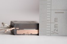
The first image is the one I posted yesterday. I include it here for completeness. It shows the copper DAP (reddish metal), the IC die (light gray), and plastic mold compound (dark gray). This cut was done along the A-A' line shown in the diagram in the final image.
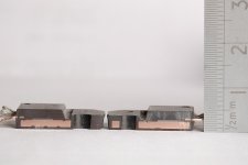
The second image shows the two halves of the package. Again the A-A' cut. It's pretty clear that the area around the mounting hole is missing some copper, at least in one of the halves.
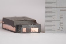
The third image shows the cross-section of the package when cut along the B-B' line. This is "horizontally" through the tab. It's pretty clear that the copper DAP is in several pieces.
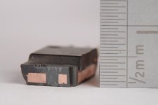
The fourth image shows the other half of the package when cut along the B-B' line.
It's pretty clear that the dominant heat flow will be from the die through the DAP to the back side of the package. In case a clamping bar is used, some heat will flow from the die to the clamping bar through the plastic. However, the thickness of the plastic from the top of the die to the top of the package is nearly four times greater than the thickness of the plastic from the DAP to the back of the package. I highly doubt the clamping bar will provide any meaningful reduction of the thermal resistance.
~Tom
Attachments
I see a few concerns there. Firstly 1D head transfer. I do not see how that is valid for a chip the size of the LM3886. More heat will go 'straight out the bottom' than out the tab. You need a 2D analysis to get an accurate estimation.
Secondly, after all this work even if you are right you are no better off than using a T package and a good washer straight onto a seat sink
Thirdly no one has given operating conditions for 100W continuous dissipation. The spec sheet states that you need at least 45V rails for that condition into 4 ohms, which is a bonkers operating point unless you are just doing it for lolz. Not an 'endurance' operating point.
Thank you for your comments, billshurv.
Re. your first concern: I disagree. We have a piece of metal (high thermal conductivity) embedded into a layer of epoxy with a much lower conductivity. In such a configuration, most of the heat will flow along the metal part, and I don't expect the 2D effects to be prominent. In other words, I expect the metal plate within the chip to be nearly isothermal.
Re. your second concern: I quite agree with you, but this is not the point in this discussion. I entered it because of the claims that the 2K/W figure can not be changed by altering the cooling surface geometry. And even in the case of the T package, clamping the tab will result in a lower die temperature, which should not be a bad thing.
Ditto for the third one: I have not discussed the operating point of the chip. The test my colleague made was to prove that dissipating 100W without frying the chip is possible, i.e. that improved cooling is possible by enclosing the chip within a metal block.
Regards,
Braca
I wonder how much copper is actually between the LM3886 IC and the back of the package. Stay tuned.
~Tom
~Tom
Seems like an : "how many angels on the head of a pin" issue.
My Update my Dynaco 3886 'kit' gut & rebuild of a Geriatric Dyna ST120.
Using the simple stoopid 1/4" ali plate OEM Dynaco heatsinks .
Do not even get warm ... on ~70 V rails. I mean I can barely feel Any heat at all
Even when left on overnight...inadvertently, after an overserving of Wine🙂
Why is this an issue elsewhere?
- Status
- Not open for further replies.
- Home
- Amplifiers
- Chip Amps
- LM3886 Thermal Experiment (with data)