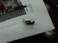
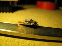
Just ruined one LM3886TF for you guys … Think a bit about your claims …
Thickness of epoxy from back side is about 0.5mm and from front side about 1mm …
I'm sorry Tom …
The final stage of our proof will be controlled experiment … Just be patient …
Thickness of epoxy from back side is about 0.5mm and from front side about 1mm …
I'm sorry Tom …
The final stage of our proof will be controlled experiment … Just be patient …
Attachments
Last edited:

The thermal resistances for the LM3886 are:
LM3886T (non-isolated): 1 K/W
LM3886TF: 2 K/W
The latter is found in the BPA200 application note (AN-1192): http://www.ti.com/lit/an/snaa021b/snaa021b.pdf
Your pictures show the isolated LM3886TF package. Its thermal resistance is 2 K/W. Do the math. If you can get 165-2*100 to be anything other than -35, I'd be most interested.
~Tom
The final stage of our proof will be controlled experiment … Just be patient …
Good luck with that. An experiment cannot prove anything. An experiment can show support for a theory or fail to show for support for a theory. That's fundamental science.
I'm looking forward to seeing your data.
~Tom
Just ruined one LM3886TF for you guys … Think a bit about your claims …
Thickness of epoxy from back side is about 0.5mm and from front side about 1mm …
I'm sorry Tom …
The final stage of our proof will be controlled experiment … Just be patient …
I don't see the 1mm from the front side, only 1mm on the tab, which is not the die. So nothing credible. Plenty incredible. I await your results but not holding your breath.
I don't see the 1mm from the front side, only 1mm on the tab, which is not the die. So nothing credible. Plenty incredible. I await your results but not holding your breath.
I agree. If the thickness on the back is 0.5 mm, the thickness between the die and the top of the package (where it connects with the clamping gizmo) looks to be at least 3 mm.
It does look like someone's cherry picking their data to match their preconceived option.
~Tom
Warning: Science content!
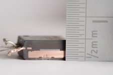
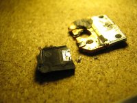
Attached is an image of the cross-section of an LM3886. I took the LM3886TF and cut it in half with a hacksaw. I then polished it up with 400 grit sandpaper. The LM3886 was cut from a PCB, which led to the shortened leads.
The copper DAP is clearly visible (reddish metal). The light gray rectangle is the IC die. The dark gray is the plastic mold compound of the IC package. Copper dust from the sanding process has smeared across the plastic mold compound. The plastic does not have copper in it.
The thickness of the mold compound measures about 0.6 mm from the DAP to the back side of the package. From the top of the die to the top of the package, the mold compound thickness is 2.2 mm. Both measured using an electronic slide caliper.
The machinist ruler included in the picture as a scale indicator has gradations every 0.5 mm. The long line on the ruler near the top of the image, with the "1" next to it, marks 1 cm.
~Tom
Attachments
Last edited:
 !!!
!!!Yes, I thought I'd say it again since the OP seemed to have missed it and appeared to think that you can always get the die cold by using a big enough heatsink. Which is not true of course - there's alway the T-difference between die and heatsink ...
")
So for 100W and 2K/W that difference is 200 degrees when dissipating 100W. To get the die below 165 degrees the heatsink must be below -35 no matter how big or fancy ....
Jan
Last edited:
No problem.
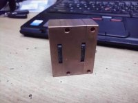
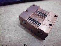
Will see does this parts and whole implementation have 2K/W, that is only important question here. Will not talk about price or practical realization, it is out of this scope.
Macola call this parts "transient heat sink" and it is made from "electro-technical copper", material used usually for making electrodes for Electrical Discharge Machining - EDM, means very high purity in a range of 99.9% or more.
Attachments
Last edited:
How do you plan to measure the difference between the "conventional" Rth j-s to compare to your special case of Rth j-s||Rth j-front-s?
Your original test was for the clamp sink to only contact the front face, leaving air as the cooling medium for the metal back plate. You could add 4.5mm of thermal insulation to the back plate and hope that the error this introduces leaves you with a result you can interpret as Rth j-front-s
Your original test was for the clamp sink to only contact the front face, leaving air as the cooling medium for the metal back plate. You could add 4.5mm of thermal insulation to the back plate and hope that the error this introduces leaves you with a result you can interpret as Rth j-front-s
>>> Your original test was for the clamp sink to only contact the front face, leaving air as the cooling medium for the metal back plate.
No no, you probably get me wrong. That is really impossible to work.
This parts MUST be mounted on additional heat sink.
PS: I'm sorry for no so good written english language. You need to understand that english language is not my native language as yours.
No no, you probably get me wrong. That is really impossible to work.
This parts MUST be mounted on additional heat sink.
PS: I'm sorry for no so good written english language. You need to understand that english language is not my native language as yours.
No problem.
Will see does this parts and whole implementation have 2K/W
That 2K/W is inside the chip package, from die to (isolation) tab - you cannot change that.
Jan
@jan.didden
I respect all you opinions and it s true what you says.
But here we have whole IC/package "trapped" inside those metal parts and for such case there is no official technical specification. That is a problem which leads to different opinions.
I would not start this whole "story" until a man who made this didn't practically tried that.
Last edited:
@jan.didden
I respect all you opinions and it s true what you says.
But here we have whole IC/package "trapped" inside those metal parts and for such case there is no official technical specification.
But also no way for the laws of thermodynamics to be bypassed. Or even an operating case that will get the device dissipating 100W continuously.
@jan.didden
I respect all you opinions and it s true what you says.
But here we have whole IC/package "trapped" inside those metal parts and for such case there is no official technical specification. That is a problem which leads to different opinions.
I would not start this whole "story" until a man who made this didn't practically tried that.
No offense meant but you don't understand what we are saying. You are like the guy who is strengthening a single chink in a chain in the hope that the chain is getting stronger.
There are many thermal resistances in what you are doing. From die to package, from package to heatsink, from heatsink to air. You can do a lot on the last two but you cannot change the first one. So the total sum of all thermal resistances can never be lower than from die to package, even with infinite heatsink and infinite good contact between package and heatsink.
Try to understand what we are saying.
Jan
Last edited:
why everyone forgets front side part where screw goes? could this be place of lower thermal resistance?
edit: isnt die to case measured only on back side?
edit: isnt die to case measured only on back side?
Attachments
Last edited:
How do you plan to measure the difference between the "conventional" Rth j-s to compare to your special case of Rth j-s||Rth j-front-s?.............
Must be my mistake.>>> Your original test was for the clamp sink to only contact the front face, leaving air as the cooling medium for the metal back plate.
No no, you probably get me wrong. That is really impossible to work.
This parts MUST be mounted on additional heat sink.
PS: I'm sorry for no so good written english language. You need to understand that english language is not my native language as yours.
So I come back to:
]How do you plan to measure the difference between the "conventional" Rth j-s to compare to your special case of Rth j-s||Rth j-front-s?
Well, I did my physics and my maths, and here are the results.
There is a fundamental flaw in applying the 2K/W figure to the copper cooling block case because, scientifically speaking, the laws of similarity are thus violated. This refers in particular to the geometrical similarity; and I hope that the simplified analysis below, which is based on first principles, will throw more light onto this problem.
Assuming an one-dimensional conduction heat transfer case, and fixing the temperature difference between the source (the die) and the heat sink surface, the amount of heat transfered is proportional to the thermal conductivity [W/m K] (a physical property of the heat transfer path) and the contact area, and inversely proportional to the distance between the source and the sink. The thermal resistance quoted in the data sheets is a composite parameter that embodies all three above mentioned quantities.
Now, since the distance between the die and the face and rear surfaces is approximately the same, and assuming that the thermal conductivity is, in the first approximation, equal in both directions, thermal resistance in the cooling block case is more than twofold of its rear surface counterpart (the two side surafces also partake in the heat transfer), reducing thus the thermal resistance by a factor of two. In that case, a temperature difference of 100K between the die and the block indeed transfers 100W, i.e. it makes use of the most of the 125W figure quoted in the 3886 DS.
One could possibly argue that the face surface is exposed to the ambient air in the standard arrangement, and thus also contributes to the 2K/W figure. While it is true that the face surface is also cooled, the prevailing heat transfer mechanism in that case is natural convection; and its thermal resistance would probably be at least an order of magnitude higher than the one between the block and the face surface.
In summary, the two cases (heat sink at the rear surface, and the cooling block) are not geometrically similar, which invalidates the application of the figure of 2K/W to the cooling block case. Due to the twice as large heat transfer area in the latter case, thermal resistance of the whole setup is also higher by the same factor.
I hope this helps.
Regards,
Braca
Last edited:
- Status
- This old topic is closed. If you want to reopen this topic, contact a moderator using the "Report Post" button.
- Home
- Amplifiers
- Chip Amps
- LM3886 Thermal Experiment (with data)