Just be patient guys ...
I preparing surprise for you, "corpus delicti" for "clamping gizmo" 😉
Probably in next 10 days as expecting one tim member to become available …
I preparing surprise for you, "corpus delicti" for "clamping gizmo" 😉
Probably in next 10 days as expecting one tim member to become available …
Last edited:
The die is connected to the DAP with a method that provides very low thermal resistance. It has to be to survive the max dissipated power listed in the data sheet.
I don't know for sure if epoxy is used or if the die is attached with that scrubbing method you describe.
The point I was trying to make was that the thermal resistance from the die, through the DAP, to the heat sink will be significantly lower than that through the plastic to the clamping gizmo to the heat sink. Hence, the thermal resistance will be dominated by that from the die through the DAP to the heat sink, and the clamp has no meaningful effect.
I suppose we could dissolve the package in hot nitric acid and figure out which die attach method was used... 🙂
~Tom
We all agree about the upper path being useless.
Power die are always attached using solder, gold tin eutectic, or gold silicon eutectic. Thermal epoxies don't have adequate thermal conductivity, solder is typically 20 times better than epoxy.
Epoxy also has a power cycle limitation as a die attach material. Given the thermal drop across the epoxy thickness, the chip on top will expand far more than the copper plate under, and this really stresses the chip to epoxy bond in a shear mode. Epoxy to metal bond strength in shear mode through cyclic fatigue between room temp and 80 to 100 C is not something you'd want to hang your hat on.
jn
We all agree about the upper path being useless.
Yep.
Power die are always attached using solder, gold tin eutectic, or gold silicon eutectic. Thermal epoxies don't have adequate thermal conductivity, solder is typically 20 times better than epoxy.
Epoxy also has a power cycle limitation as a die attach material. Given the thermal drop across the epoxy thickness, the chip on top will expand far more than the copper plate under, and this really stresses the chip to epoxy bond in a shear mode. Epoxy to metal bond strength in shear mode through cyclic fatigue between room temp and 80 to 100 C is not something you'd want to hang your hat on.
That makes sense. Thanks for providing some insight (and facts ... concept! 🙂) I enjoy reading your posts.
~Tom
We all agree about the upper path being useless.
Except me and my colleague Macola!
Except me and my colleague Macola!
If you can provide data to support the assertion that the epoxy path above the chip is worth anything, that'd be interesting.
Having worked in the industry, actually soldering power dice onto copper baseplates, then wirebonding them, then glob top die coating to protect the die from the encapsulation epoxy, then either injection molding (very common), or epoxy encapsulating the structure, I am quite familiar with all the materials, processes, and designs for this type of device.
As I was also responsible for thermal testing of this type of assembly, I am also well versed in the equipment needed for this testing, as well as the ramifications of the various methods of cooling these chips.
What you propose is inconsistent with my experience. As I recall, the test methodology you mentioned was not suitably controlled.
It would be great to actually have a temperature dependent parameter on the silicon which could be used to actually measure the die temperature. To attempt to do so externally using constant power is useless, as you cannot determine the rise in junction.
jn
@jneutron
I will try to provide as much as I can information on that matter. I hope it will be useful for everyone.
We will organize and setup relevant test and provide results in written form.
One of our tim member who will arrive here in next 10 days is doctor of science and professor with very large practical experience in thermo dynamics and we will follow it's advices to prepare and conduct valid test.
Believe me this is not a joke and man behind this idea knows very well what they are doing.
Nice.@jneutron
I will try to provide as much as I can information on that matter. I hope it will be useful for everyone.
We will organize and setup relevant test and provide results in written form.
One of our tim member who will arrive here in next 10 days is doctor of science and professor with very large practical experience in thermo dynamics and we will follow it's advices to prepare and conduct valid test.
Believe me this is not a joke and man behind this idea knows very well what they are doing.
From the earlier description, it looked like you were seeing the result of a larger copper to water interface, not necessarily a result of better chip to world interface.
Have the PhD chap look for a metric for die temperature. It may be possible to use a diffusion tub forward biased to measure die temp. The circuits on these chips are generally isolated from the substrate by reverse biased pn junctions, so if you guys could find one of those from one of the leads to the outside world, then half the work is done.
A simple IR camera may also be of help here. If you can see that the top copper actually has a higher temp directly over the center of the package, that would only be explained by thermal transfer through the top. If the top copper is simply spreading the bottom copper heat upwards, then you should see the top center as lower temp than the side areas.
Good luck with the test. Keep us posted.
jn
Have the PhD chap look for a metric for die temperature.
+1
One DIY way to estimate the die temperature is to track the voltage on the MUTE pin. You'll have to calibrate at some known temperature as the "temperature sensor" is a Vbe stack with a couple of resistors (that probably have their own tempco as well).
~Tom
+1
One DIY way to estimate the die temperature is to track the voltage on the MUTE pin. You'll have to calibrate at some known temperature as the "temperature sensor" is a Vbe stack with a couple of resistors (that probably have their own tempco as well).
~Tom
Tnx for useful info.
+1
One DIY way to estimate the die temperature is to track the voltage on the MUTE pin. You'll have to calibrate at some known temperature as the "temperature sensor" is a Vbe stack with a couple of resistors (that probably have their own tempco as well).
~Tom
hm , could you provide more detail on this , or where to find details.
and what is tempco?
would this method be precise enough?
"tempco" could mean either of: TEMPerature COmpensation, or TEMPerature COefficient.
The context within the sentence will usually make clear which is intended.
The context within the sentence will usually make clear which is intended.
+1
One DIY way to estimate the die temperature is to track the voltage on the MUTE pin. You'll have to calibrate at some known temperature as the "temperature sensor" is a Vbe stack with a couple of resistors (that probably have their own tempco as well).
~Tom
Nice information. Thank you.
jn
hm , could you provide more detail on this , or where to find details.
I suggest looking at the equivalent circuit schematic for the LM3886 on page 7 in the data sheet.
and what is tempco?
Tempco = Temperature coefficient.
would this method be precise enough?
Depends on how good your calibration is... The tempco is dependent on the doping concentrations and doping profiles of the various semiconductors. These will shift slightly as a function of process variation. The tempco is generally very reliable, but the absolute value of the PN junction forward drop varies widely, hence the need for calibration.
~Tom
Most do us have probably experienced the warmup process and change in sound. Has anyone figured what die temperature range is optimum?
You have to draw >500uA from the Mute pin to turn on fully. The voltage will be about -2V and reduce by about 6mV/C
Nice, thanks.You have to draw >500uA from the Mute pin to turn on fully. The voltage will be about -2V and reduce by about 6mV/C
Is it possible to monitor the mute pin while the device is delivering power to the load? Or, does the audio signal also affect the mute voltage.
If they interact, one can use a duty cycle on the device. 99% on time, 1% off time, and during off, monitor the mute voltage.
The entire structure has several time constants. The top to bottom of the chip will be in the 100 uSec to 1 millisecond timeframe, the chip to heatsink will be in the 1 to 10 second area.
When you stop the drive, the mute voltage will be consistent with the die bottom temperature within the 100 uSec timeframe, and will track it's copper in the second or so timeframe. As you experiment, you will be able to spot the time constants.
Note: I assume that there are no electrical time constants involved in the mute circuitry, but have no idea.
jn
You are right, physics and math don't lie, BUT just one small piece of information here is missing or unknown to you, and that is "thermal resistance" with this cooling method 🙂
That doesn't matter. If the thermal R from die to heatsink is 2K/W and it dissipates 100W, the temp diff between die and heatsink is 200 degrees.
If the max die temp is 165 C for the protection to kick in, the heatsink temp MUST be not higher than -35 C. Whatever the thermal R of the heatsink is.
Jan
That doesn't matter. If the thermal R from die to heatsink is 2K/W and it dissipates 100W, the temp diff between die and heatsink is 200 degrees.
If the max die temp is 165 C for the protection to kick in, the heatsink temp MUST be not higher than -35 C. Whatever the thermal R of the heatsink is.
Gee... That sounds familiar: Post #222. 🙂
~Tom
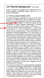
The same information can be found in "National Application Specific Analog Product Databook" published in 1995 … If you have it …
Also more useful info can be found there in opposite to current TI's DS.
I told you guys that we are in analog electronic fields for very long time …
Attachments
Last edited:
- Status
- Not open for further replies.
- Home
- Amplifiers
- Chip Amps
- LM3886 Thermal Experiment (with data)