Simple circuits always sounds nice
I am happy to see you in activity dear Sheldon.
regards,
Carlos
I am happy to see you in activity dear Sheldon.
regards,
Carlos
Thanks Carlos and Hugh.
To answer this and Nelson's question, I'm gonna have to pick up a signal generator and learn how to use the scope I have sitting here. Too much good stuff. Plus a couple more variations to try here.
Sheldon
AKSA said:How much power?
To answer this and Nelson's question, I'm gonna have to pick up a signal generator and learn how to use the scope I have sitting here. Too much good stuff. Plus a couple more variations to try here.
Sheldon
Hi Sheldon,
Great to see all the progress you've made & good to hear that it's so worthwhile sonically. Would love to hear more about the sonics when you are comfortable with the configuration.
I'm still waiting on delivery of Tix solder before I can get started, Ordered it about 2 weeks ago from here www.micromark.com
Hi Sheldon,
Nice pics of the hardware, thanks.
The zeners are there to protect against over voting the gate with respect to source/drain.
For the LU1014D these are:
Drain-Source Voltage VDS 24V
Gate-Source Voltage VGS -12V
Gate-Drain Voltage VGD -28V
Because the input transformer's secondary isn't constrained by any power rails it is easy to inadvertently exceed these limits.
I have done this several times myself in the past, and for parts like the IRFP150s it was a one shot failure (and why I got the habit of using a fuse in the DC supply line AFTER the storage cap).
You could try increasing the zener voltage a bit to reduce the effect it seems to be having. Looking at the figures though I would not go beyond 6 volts as you really don't want to exceed that VGD figure (the part will avalanche).
Hope your weekend has been productive.
Best wishes,
Susan.
Nice pics of the hardware, thanks.
Sheldon said:The zeners were supposed to provide some protection against killing the FET with too much voltage swing. I actually just removed them, as they conduct enough to upset the bias a bit.
The zeners are there to protect against over voting the gate with respect to source/drain.
For the LU1014D these are:
Drain-Source Voltage VDS 24V
Gate-Source Voltage VGS -12V
Gate-Drain Voltage VGD -28V
Because the input transformer's secondary isn't constrained by any power rails it is easy to inadvertently exceed these limits.
I have done this several times myself in the past, and for parts like the IRFP150s it was a one shot failure (and why I got the habit of using a fuse in the DC supply line AFTER the storage cap).
You could try increasing the zener voltage a bit to reduce the effect it seems to be having. Looking at the figures though I would not go beyond 6 volts as you really don't want to exceed that VGD figure (the part will avalanche).
Hope your weekend has been productive.
Best wishes,
Susan.
I am sure Nelson knows what the Zener's are meant to be there for. I guess he was giving a hint on 3V being too low (so that they leak too much at normal operating voltages). I myself uses something around 8V. Same probably also applies to his question about the 200R gate resistor. If I am not wrong, the effective input capacitance of the cascoded JFET used as a follower is very low. With my limited experience with the LU1014s, they do tend to oscillate quite a bit. On a Id vs Vgs test setup, I have to use up to 1k gate resistor to stop oscillation.
Hope you are keeping well, Susan.
(I have not been making much progress of late. Changing circuits and mechanical layouts too many times.)
🙂
Cheers,
Patrick
Hope you are keeping well, Susan.
(I have not been making much progress of late. Changing circuits and mechanical layouts too many times.)
🙂
Cheers,
Patrick
Thanks Susan and Patrick. I haven't any practical experience with these FET's or many Zeners, for that matter. I suspected that the 3V devices might be leaking more than higher voltage versions. I have some 5V units and higher on hand, and they are simple enough to try. I'll see how high I need to go to not affect the balance too much. Without the current zener, the secondary halves are balanced within about 5mA. No problem trying higher gate stopper either, so if there is no real down side, I see no reason not to go with something around 1K.
Thanks for reminding me about the fusing Susan. I'll keep that in mind when I assemble into a chassis.
Sheldon
P.S. Spent the weekend herding grandsons. So, while busy, not a lot of soldering going on.
Thanks for reminding me about the fusing Susan. I'll keep that in mind when I assemble into a chassis.
Sheldon
P.S. Spent the weekend herding grandsons. So, while busy, not a lot of soldering going on.
Ok, got back to the bench. Changed the zeners to 5V versions and just for good measure changed the gate stoppers to 1K. That seems to be fine. Offset in worst case is about 8mA.
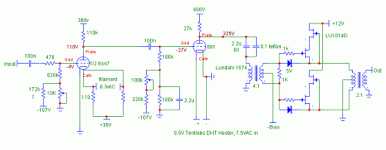
So, not content to stop there, I reversed the wiring on the input transformer and drove it with a tube section as shown below. Seems to work fine, but no extensive listening tests. The Lundahl 1674 is a 1/1:4/4. I need to do that to get a center tap on the secondary. Would like to try 8:1. Wonder if I couldn't parallel the secondaries and use a resistor divider as a virtual center tap?
Sheldon
edit: error in schema
Attachments
EUVL said:I am sure Nelson knows what the Zener's are meant to be there for.
Actually I don't see why they're there. If this were a Mosfet, we
would need to protect the Gate oxide insulator. There is no
insulator on the JFET, and I don't think we're likely to damage
the Gate.
😎
Mr. Pass,
I think Sheldon replaced the mosfets, as originally designed by Susan, with cascoded jfets and did not realize the zeners are no longer needed.
I think Sheldon replaced the mosfets, as originally designed by Susan, with cascoded jfets and did not realize the zeners are no longer needed.
> There is no insulator on the JFET, and I don't think we're likely to damage the Gate.
I thought I remember seeing an absolute rating of Vgs at -12V and Vgd at -28V on the datasheet. No need to make sure that they are not exceeded ?
Patrick
I thought I remember seeing an absolute rating of Vgs at -12V and Vgd at -28V on the datasheet. No need to make sure that they are not exceeded ?
Patrick
JFET Protection
Dear All,
Whilst I concur that the gate protection requirements of MOSFETs are not the same as with the JFETs I still think it is better to be safe and ensure that the various maximum operating voltages are not exceeded.
"Design for failure, plan for success."
I regret that I don't have any of these parts to bench test (my budget isn't up to getting anything that I am not specifically able to use in my own system) so my comments are theoretical.
Mr Pass has used these parts as he so kindly details in his Zen Variations #8 and #9.
<< I assume you have not had any problems from exceeding device maximums (beyond the obvious in Figs 4 and 5)? >>
Note however that the cascode is for a gain stage, not a follower.
=============
Looking at the Lovoltech (now QSpeed) application notes
http://www.qspeed.com/
(Register to get access to the technical info.)
See AN103: Avalanche Testing for Power JFETs
Which describes a test set-up. This isn't how we are using the parts, so the test as described does not really translate into our circuit operation. However it does describe avalanche effect.
If the part can be tripped into avalanche conduction it may not completely lock up the part as it would in a MOSFET. However it is still likely to have noticeable effects on the output which is undesirable.
To quote from AN108: Using JFETs in Low-Side apps.pdf
"The Power JFET gate circuit differs from the MOSFET in two significant ways. The MOSFET uses gate oxide, to blocks any DC path through the gate. The JFET gate consists of a Gate-Source junction. In the forward direction, the Gate-Source diode clamps VGS to 0.7V."
"The MOSFET is an enhancement mode device, and turns on only when there is prohibitive VGS. The JFET is a depletion mode device, which means that the channel is on until VGS is negative (the gate-source junction is reverse biased)."
So the desired thing is to prevent excessive Gate-Drain Voltage (VGD -28V) which in this instance could be accomplished by connecting a 27V zener between the gate and drain of the input device. The capacitive effects of the zener is reduced as the Drain is moving as well due to the cascode.
Best wishes,
Susan.
Dear All,
Nelson Pass said:Actually I don't see why they're there. If this were a Mosfet, we would need to protect the Gate oxide insulator. There is no insulator on the JFET, and I don't think we're likely to damage the Gate.
Whilst I concur that the gate protection requirements of MOSFETs are not the same as with the JFETs I still think it is better to be safe and ensure that the various maximum operating voltages are not exceeded.
"Design for failure, plan for success."
I regret that I don't have any of these parts to bench test (my budget isn't up to getting anything that I am not specifically able to use in my own system) so my comments are theoretical.
Mr Pass has used these parts as he so kindly details in his Zen Variations #8 and #9.
<< I assume you have not had any problems from exceeding device maximums (beyond the obvious in Figs 4 and 5)? >>
Note however that the cascode is for a gain stage, not a follower.
=============
Looking at the Lovoltech (now QSpeed) application notes
http://www.qspeed.com/
(Register to get access to the technical info.)
See AN103: Avalanche Testing for Power JFETs
Which describes a test set-up. This isn't how we are using the parts, so the test as described does not really translate into our circuit operation. However it does describe avalanche effect.
If the part can be tripped into avalanche conduction it may not completely lock up the part as it would in a MOSFET. However it is still likely to have noticeable effects on the output which is undesirable.
To quote from AN108: Using JFETs in Low-Side apps.pdf
"The Power JFET gate circuit differs from the MOSFET in two significant ways. The MOSFET uses gate oxide, to blocks any DC path through the gate. The JFET gate consists of a Gate-Source junction. In the forward direction, the Gate-Source diode clamps VGS to 0.7V."
"The MOSFET is an enhancement mode device, and turns on only when there is prohibitive VGS. The JFET is a depletion mode device, which means that the channel is on until VGS is negative (the gate-source junction is reverse biased)."
So the desired thing is to prevent excessive Gate-Drain Voltage (VGD -28V) which in this instance could be accomplished by connecting a 27V zener between the gate and drain of the input device. The capacitive effects of the zener is reduced as the Drain is moving as well due to the cascode.
Best wishes,
Susan.
Susan,
If you fancy a couple of LU1014s to try, drop me a private email. My pleasure.
🙂
Patrick
If you fancy a couple of LU1014s to try, drop me a private email. My pleasure.
🙂
Patrick
Hi Patrick,
You got you post in whilst I had started a reply, then was meandering through application notes and data sheets which, looking at the time now, I see took well over an hour.
Yes, quite.
Hence my "Design for failure, plan for success." comment.
The Zeus circuit is very robust and can survive a lot of incidents, as long as the (MOS)FET maximums are not exceeded.
One scenario is having the preamp/line driver operating and the power amp not yet turned on.
With MOSFETs there is enough of a direct connection that sound, albeit low and distorted, will come out speakers even when the power stage is not powered up.
Without zeners the maximum gate voltages are easily exceeded, and could cause a situation where avalanche occurred on turn on as the supply rail comes up.
For me a significant part of design and one that often seems to take the majority of the time is working to ensure reliable operation under ALL operating conditions.
Best wishes,
Susan.
You got you post in whilst I had started a reply, then was meandering through application notes and data sheets which, looking at the time now, I see took well over an hour.
EUVL said:I thought I remember seeing an absolute rating of Vgs at -12V and Vgd at -28V on the datasheet. No need to make sure that they are not exceeded ?
Yes, quite.
Hence my "Design for failure, plan for success." comment.
The Zeus circuit is very robust and can survive a lot of incidents, as long as the (MOS)FET maximums are not exceeded.
One scenario is having the preamp/line driver operating and the power amp not yet turned on.
With MOSFETs there is enough of a direct connection that sound, albeit low and distorted, will come out speakers even when the power stage is not powered up.
Without zeners the maximum gate voltages are easily exceeded, and could cause a situation where avalanche occurred on turn on as the supply rail comes up.
For me a significant part of design and one that often seems to take the majority of the time is working to ensure reliable operation under ALL operating conditions.
Best wishes,
Susan.
Hi Patrick,
Ha, another "whilst I was writing a reply" post!
Thanks for the offer, will be in touch.
Best wishes,
Susan.
Ha, another "whilst I was writing a reply" post!
EUVL said:Susan, If you fancy a couple of LU1014s to try, drop me a private email. My pleasure.
Thanks for the offer, will be in touch.
Best wishes,
Susan.
Hi Sheldon,
In general for the standard Zeus circuit it is quite possible to use a resistive divider.
My experience is that THD% distortion is a little worse compared to using a center tap.
However I would need to do some AB testing to give an absolute on this as it may well be a difference in even harmonics which is not really a problem.
With the apparent gate current issue, it may not be so straightforward an issue with the JFETs.
Looking at the data sheet:
http://www.lundahl.se/pdfs/datash/1674.pdf
The DC (Static) resistance of each primary (which is the secondary in your configuration) of the Lundahl 1674 is specified as 33 ohms, however you would (I assume) be using a much higher resistance for the virtual center tap?
Best wishes,
Susan.
Sheldon said:So, not content to stop there, I reversed the wiring on the input transformer and drove it with a tube section as shown below. Seems to work fine, but no extensive listening tests. The Lundahl 1674 is a 1/1:4/4. I need to do that to get a center tap on the secondary. Would like to try 8:1. Wonder if I couldn't parallel the secondaries and use a resistor divider as a virtual center tap?
In general for the standard Zeus circuit it is quite possible to use a resistive divider.
My experience is that THD% distortion is a little worse compared to using a center tap.
However I would need to do some AB testing to give an absolute on this as it may well be a difference in even harmonics which is not really a problem.
With the apparent gate current issue, it may not be so straightforward an issue with the JFETs.
Looking at the data sheet:
http://www.lundahl.se/pdfs/datash/1674.pdf
The DC (Static) resistance of each primary (which is the secondary in your configuration) of the Lundahl 1674 is specified as 33 ohms, however you would (I assume) be using a much higher resistance for the virtual center tap?
Best wishes,
Susan.
Re: JFET Protection
Thanks for the replies all. And this all happens while I sleep. Gotta love it. As I know very little about failure modes for these devices, I was just trying to avoid exceeding the published maximum values. None of them would be exceeded by driving the amp with my current pre-amp, as I can set the maximum output voltage swing. I was actually more concerned about using a tube based driver stage, and in that case, I can exceed the Vgs and maybe Vgd. I don't know if these maximums refer to steady state conditions or to even very short duration swings, so was trying to be on the safe side.
Thanks Susan. This is one of those things that is easy and safe enough to try. Just was curious as to limitations. The loadline on the 801 as set up with OPT's, is about 8K (27K//12K). As long as the transformer doesn't mind, I don't guess that it would be problem to decrease the load, may even lower distortion. So at 8:1, a divider pair with a total of around 200 Ohms would give a reflected load of 12.8K. Could increase the resistance from there too.
Sheldon
Susan-Parker said:o the desired thing is to prevent excessive Gate-Drain Voltage (VGD -28V) which in this instance could be accomplished by connecting a 27V zener between the gate and drain of the input device. The capacitive effects of the zener is reduced as the Drain is moving as well due to the cascode.
Thanks for the replies all. And this all happens while I sleep. Gotta love it. As I know very little about failure modes for these devices, I was just trying to avoid exceeding the published maximum values. None of them would be exceeded by driving the amp with my current pre-amp, as I can set the maximum output voltage swing. I was actually more concerned about using a tube based driver stage, and in that case, I can exceed the Vgs and maybe Vgd. I don't know if these maximums refer to steady state conditions or to even very short duration swings, so was trying to be on the safe side.
Susan-Parker said:[Bn general for the standard Zeus circuit it is quite possible to use a resistive divider.
My experience is that THD% distortion is a little worse compared to using a center tap.
However I would need to do some AB testing to give an absolute on this as it may well be a difference in even harmonics which is not really a problem.
With the apparent gate current issue, it may not be so straightforward an issue with the JFETs.
Looking at the data sheet:
http://www.lundahl.se/pdfs/datash/1674.pdf
The DC (Static) resistance of each primary (which is the secondary in your configuration) of the Lundahl 1674 is specified as 33 ohms, however you would (I assume) be using a much higher resistance for the virtual center tap? [/B]
Thanks Susan. This is one of those things that is easy and safe enough to try. Just was curious as to limitations. The loadline on the 801 as set up with OPT's, is about 8K (27K//12K). As long as the transformer doesn't mind, I don't guess that it would be problem to decrease the load, may even lower distortion. So at 8:1, a divider pair with a total of around 200 Ohms would give a reflected load of 12.8K. Could increase the resistance from there too.
Sheldon
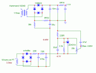
One problem with the amp as set up with a simple bias supply, is that at the temperature of the heat sink rises, the bias goes up. In my case, with only the structure shown above, if I started at about 300mA bias per side, it would rise to about 400mA until it reached equilibrium at around 50-60 degrees C. So, I cooked up the following scheme. The resistor on the return leg of the main supply gives a negative reference for the bias supply which counteracts the increase in current. With the dropping resistor value shown, if I set the bias at 400mA, it rises to about 430mA at equilibrium. If I use a slightly larger resistor, such that the drop is about equal to the bias voltage at the set current, there is no change at all.
It's a bit interactive, so you have to decide the current set conditions first, but it seems to work fine. Values shown are taken at about 400mA bias per side.
Sheldon
It's a bit interactive, so you have to decide the current set conditions first, but it seems to work fine. Values shown are taken at about 400mA bias per side.
Sheldon
Attachments
Bias supply
Hi Sheldon,
Thanks for the temperature compensating bias supply info.
Best wishes,
Susan.
Hi Sheldon,
Thanks for the temperature compensating bias supply info.
Best wishes,
Susan.
- Home
- Amplifiers
- Solid State
- Zero Feedback Impedance Amplifiers