
so, Lamborghini style?
why simple, when we want to use whatever amount of 'Talian wire products we have on stock?

why simple, when we want to use whatever amount of 'Talian wire products we have on stock?
I'm moving ahead and rebuilding my Iron Pre in what will be it's eventual home. The case comes from an old KVM switch, courtesy of the trash at work, which is nice thick steel, comes with the holes for RCAs (or BNCs in my case) already drilled, and you get 16 standoffs for free, since they come on the old VGA sockets. The case is 17" x 6" useful space inside, so a nice convenient length but just a little narrow.
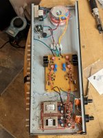
The idea is to work a sequence of iterations, perfecting as I go. The first one (in the attached photo) has the same buffer/transformer and power transformer from the temporary chassis, but has a new PSU board. I did a PCB with laser printer and etched it myself; it was the first one I'd done in years, and it needed some p2p work to correct places where the traces didn't survive the etching. (I tried two or three different sharpies to correct places where the laser printing came off, but the vingear/peroxide etching solution I used washed them all off... you live and learn.) Much shorter signal wiring in this version. Volume controls are L and R mono 20-turn wirewound pots. Next steps will be to add switched inputs, first just with a rotary switch and later maybe with relays.
It sounds great, and I'm still having loads of fun with this project. Nonetheless I've had a couple of ideas that I'm curious about.
Firstly, I'm going to try doing the power supply again; I can reuse the components, so it's only the boards that need doing. There may be potential for a little less measured noise (I can't hear any in use, so I'm not quite sure why I care, but there you are... what's more, noise as measured on REW may say more about my setup than about the preamp - still working on that.) Also, in the chassis I'm using I need to get a PSU that's narrower if I'm going to try relays on the inputs, since right now there just isn't enough space.
Secondly, it occurred to me that the overall design (as ZM describes above) are a unity gain buffer, then the autoformer for gain. Presumably the same principle could be applied to other unity gain buffers, just as it is in the M2X project. So wouldn't it be possible to use the daughter boards from that project to try out different buffers here too? If I understand correctly (there's no guarantee of that!) then T11/T12 and the couple of caps connected to them are a capacitance multiplier, and just smooth the input voltage, so these could be on the motherboard together with the transformers, and you could drop in the daughter card with connections at the four standoffs, just like in the M2X. Just to be clear; I have no reason to think other buffers would sound better, just that it sounds like fun to try them out.
Thoughts?
Best
Nigel
Attachments

These have been fun so far, for sure.all roads are leading to Rome
just take care to choose fun ones

in the end, you can use OP for buffer there, and that one should be most invisible
not disputing that approach at all ( in fact Mighty ZM going to sin big, in INT, with OPA1632) .... but that wasn't fun in that time and space point
not disputing that approach at all ( in fact Mighty ZM going to sin big, in INT, with OPA1632) .... but that wasn't fun in that time and space point
Sorry if I'm being dim, but what does OP mean here? OutPut? Original Post?in the end, you can use OP for buffer there, and that one should be most invisible
not disputing that approach at all ( in fact Mighty ZM going to sin big, in INT, with OPA1632) .... but that wasn't fun in that time and space point
Actually, I don't think I know what INT means, either... Maybe I'm slow this morning?
I think I have a couple OPA1632 in my parts box. (No idea why.)
I think I have a couple OPA1632 in my parts box. (No idea why.)
OP means Operational amplifier
see Tombo's buffer for LuDEF and similar ones
regarding INT, I posted somewhere teaser of planed FE for integrated amp
it's called, very cleverly and innovative from my side - INT
see Tombo's buffer for LuDEF and similar ones
regarding INT, I posted somewhere teaser of planed FE for integrated amp
it's called, very cleverly and innovative from my side - INT
OK, thanks. You see, I said I was being slow this morning... 🙂 I'll think some more about the idea of daughter cards.
Hi ZM,
I have either a simple or a stupid question. Somewhere, maybe in the thread about tombo's buffer where I mentioned using the Gemini shunt reg, you commented that it could be programmed for different output voltage, and different idle current. If I recall correctly you said the SE version was programmed for 60mA idle current, and the balanced one for 100mA, or something like that. I thought that meant that some of the values in the Gemini schematic (probably R values) are different for the SE and Bal cases, but looking at posts #1149 and #1150 (which I think have the latest schematics) I can't see any difference in the values at all. Am I missing something? Or looking in the wrong place?
In the other thread you also offered to point out the correct values hat things should be changed to for specified V and I, but I'm not asking for that right now. Just asking to be pointed int he right direction...
Thanks
Nigel
tell me in which post is set of last schematics and I'll tell you how to
dunno what I said before ( remember - Pa is saying and writing all sorts of misleading facts all the time, but his neck is never on chopchop ; I did contemplated few times how I understand that habit ) but there is no reason that programmed current is different for SE and Bal iteration - in both cases one Good Gemini is feeding 2 buffer cells - for SE one Good Gemini for both channels ( on one pcb) , for Bal - one Good Gemini for both phases (of one channel on one pcb)
60 or 100mmA, no difference ....... each buffer cell drawing measly under-10mA
dunno what I said before ( remember - Pa is saying and writing all sorts of misleading facts all the time, but his neck is never on chopchop
; I did contemplated few times how I understand that habit ) but there is no reason that programmed current is different for SE and Bal iteration - in both cases one Good Gemini is feeding 2 buffer cells - for SE one Good Gemini for both channels ( on one pcb) , for Bal - one Good Gemini for both phases (of one channel on one pcb)60 or 100mmA, no difference ....... each buffer cell drawing measly under-10mA
Hmmm... I wonder if my memory is failing me worse than I thought, then...😱 I tried looking for your post, but it's been a few days, and I couldn't find it to cut and paste into my last reply here. Probably looking in the wrong thread or something...
I understand that for the Iron Pre 60mA or 100mA would make no difference, but using the Gemini elsewhere it might. (As tombo suggested it would with his buffer in the absence of the OPA551FA super regs.) In any event, if as you say the SE and Bal versions use exactly the same schematic for the Gemini then I'm looking in vain.
Maybe I could ask the question in a different way. I'm guessing that if you want to change the output voltage you change values in the resistor chain that links +V and -V, through the two trimpots. (Right?) But I can't see what you would change if you want to keep the same output voltages but want to increase the idle current. (?)
Now I think about it, I'm guessing the Iron Pumpkin needs a higher idle current, so maybe comparing the values in that thread with this one might give me a hint... hmmm...
Best
Nigel
as I said - change is trivial and sole thing you need to take care of is - what size of heatsink you need then for CCS BD transistors and shunt IRF ones
when you need it for something ( anything) particular, post schematic and give me details about intended use, then I'll explain
which I did few times already, somewhere, but even I can't remember when and where, so just don't waste time searching
edit: - just do not ask for output voltage much lesser than 12V and for, dunno, 500mA of output current ..... pcb simply isn't made for that
OK, thanks. I was just trying to understand how the reg works a little better, but I can certainly wait.
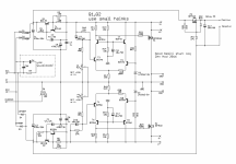
Q1T1 are input CCS, giving entire reg's programmed current; governor is T1, where programmed current is set as Vbe/(R3//R4)
after that you have LTP (T3T9) serving as error amplifier; on one input U1 is giving ref. voltage (to T9)
every error amp is having important character flaw, on which we are counting - it is doing everything to maintain Status Quo ....... in other words - same voltage level on both inputs
- T5T7 are "just" voltage umbrella for LTP
T3 is sensing output voltage through resistive divider R10R8P1, doing its hodgepodgeamplifying via R11, forcing M1 to eat what needs to be eaten , to maintan voltage at T3 base same as voltage at T9 base
resistive divider is setting ratio of voltage at T3 base and voltage above T3 base
now, I wrote 5 lines of text; I can give you in any moment 15 books about electronics which will give you 55 extra nice evenings of learning fun stuff
neither of those is hard for me, but I know which way you can learn more and have enormously more fun
- Home
- Amplifiers
- Pass Labs
- What's wrong with the kiss, boy?