What PSU are you using?I have the same issue with the VCX jumping to full volume. I emailed Lenny last week and he mentioned there is a firmware issue with one of the components, and I should email it back for it to get the new firmware flashed to solve the problem.
I tried two different VRDN boards I had and both jumped to full volume. Once I switched to a different regulated PSU the problem went away.
I never did try bypassing the denoiser though.
I never did try bypassing the denoiser though.
I need to finish my iron-pre before sending the vcx back to be flashed. That said, its a bit unnerving when the volume goes full tilt, and ear or equipment damage is a possibility. Maybe I will disable the de-noiser for now and see if the problem crops up again.

It seems like the right answer is to get the VCX flashed by getting it back to Lenny. Wouldn't hurt for starters.
The VCX is specced for 9-16VDC. If you're setting a VRDN for 18VDC or higher for the BA2018 and connecting the VCX to that same regulator, then it's likely that something could go wrong. Lenny's LPS9, for instance, supplies just 14VDC. I don't know what your configuration looks like, but I worked through those numbers when planning my own BA2018.
The VCX is specced for 9-16VDC. If you're setting a VRDN for 18VDC or higher for the BA2018 and connecting the VCX to that same regulator, then it's likely that something could go wrong. Lenny's LPS9, for instance, supplies just 14VDC. I don't know what your configuration looks like, but I worked through those numbers when planning my own BA2018.
Lenny had already sent me a replacement VCX a couple months ago but same problem. He guaranteed me they tested it and couldn’t replicate the problem and told me to try a new PSU and that worked. I guess he had a lot more people respond with the same issue so is back testing and flashing a new firmware. I just purchased another VCX a couple weeks ago and he informed me they are delayed getting them out to do this.
I’ve been setting the VRDN and my other supply at +-15V and then making the resistor changes recommended by Lenny in his App Notes. It’s just four total resistors.
I’ve been setting the VRDN and my other supply at +-15V and then making the resistor changes recommended by Lenny in his App Notes. It’s just four total resistors.
It is sold out in the store.The current BA2018 will be in the store indefinitely, as far as I know...
🙂
Coming back soon?
Thants DT
I’d assume so. There’s a bunch of completion kits on hand so only boards need reorder.
For anyone using the Muses VCX, how are you powering it? If you use, in particular, Lenny's LPS9 it requires 5Vdc, so where are you sourcing that from? I considered using the Muffsy IRM-05-5 PSU breakout board, but then that seems silly to take 120Vac, step it down to 5Vdc, then let the LPS9 step the power back up to 14Vdc. Why not just use a MeanWell IRM-05-15 transformer and power the VCX directly? Then I realized that in the chain I might gain some power regulation and reduce some noise. I dunno.
Anyway, comments appreciated!
Anyway, comments appreciated!
Hi All,
I got my power supply issues resolved with the help of some folks over at the power supplies section. I'm closing in on finishing the project. Case work is done. Power supply and signal wiring is done. I had a difficult time getting the offset to the correctly low voltage, especially on one channel. It felt like the pot was kind of twitchy and very sensitive. I did manage, though.
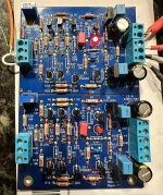
Today I hooked the board up to the unit's power, with input from a portable digital player and output going through a class D amp and a small test speaker. One half of the board seems fine: pretty good level of gain, no hiss, no hum. The other half (top in photo) has quite a bit of hiss and a lot less output. Wondering if this sounds like a familiar failure mode to anyone. The two halves of the board look identical to me, but maybe your eagle eyes will spot something. I will admit to installing one of the electrolytics (C5) on the good half backward, so that had to be replaced, which is why it looks different--same value though.
Lacking any other kind of plan, my inclination is to replace all the transistors on the bad half. I know this is not a proper test, but using a VOM, I checked resistance values between legs of the transistors in both polarities, and each measurement from the halves was in pretty good agreement, with no shorts or open circuits. Would it make sense to replace the early stage ones first and proceed to the next, or just do them all in one shot?
Any better thoughts on how to proceed? Always appreciate the wisdom and experience here.

I got my power supply issues resolved with the help of some folks over at the power supplies section. I'm closing in on finishing the project. Case work is done. Power supply and signal wiring is done. I had a difficult time getting the offset to the correctly low voltage, especially on one channel. It felt like the pot was kind of twitchy and very sensitive. I did manage, though.
Today I hooked the board up to the unit's power, with input from a portable digital player and output going through a class D amp and a small test speaker. One half of the board seems fine: pretty good level of gain, no hiss, no hum. The other half (top in photo) has quite a bit of hiss and a lot less output. Wondering if this sounds like a familiar failure mode to anyone. The two halves of the board look identical to me, but maybe your eagle eyes will spot something. I will admit to installing one of the electrolytics (C5) on the good half backward, so that had to be replaced, which is why it looks different--same value though.
Lacking any other kind of plan, my inclination is to replace all the transistors on the bad half. I know this is not a proper test, but using a VOM, I checked resistance values between legs of the transistors in both polarities, and each measurement from the halves was in pretty good agreement, with no shorts or open circuits. Would it make sense to replace the early stage ones first and proceed to the next, or just do them all in one shot?
Any better thoughts on how to proceed? Always appreciate the wisdom and experience here.
Your bias diode (led) is not lit. Lot’s of advice on troubles with these boards. 90% are due to jfet issues. Mostly because of bad solder joints.
Then ensure all BJT’s are the correct ones in the correct locations. Orientation looks OK.
A quick measure across the 10R resistors on the bad chan will reveal if the JFET CCS provide the appropriate current. If it drifts, check JFET solder joints and function.
You can do a point to point beep test before and after the JFETs and to the next point on the board. If resistance appears, resolder. If JFETs are OK, report back. They should provide approx 3mA current, measured across the 10R resistors.
You should post measured voltage drop across all the 10R resistors after the JFETs here. Also describe possible drift in voltage drop across same resistors.
The same voltage drifts or shortages will appear amplified at R7 and R13, measure there too. Perhaps the route to a working chan is short.
The usual reflowing of all suspect joints apply.
A wonderful linestage, a bit of a hassle sometimes to get up and running.
Attachments
smd - use no-clean (helper) flux
or kalophone melt/thinned with alcohol
whatever handy to help soldering little buggers
or kalophone melt/thinned with alcohol
whatever handy to help soldering little buggers
Haha, sorry for my bad eye.
To emphasize the point: jfet troubles can also be measured across circled resistors, when circuit is on. And also through continuity checks off. You’ll get it right.
To emphasize the point: jfet troubles can also be measured across circled resistors, when circuit is on. And also through continuity checks off. You’ll get it right.
6L6, do you mean the whole transistor is bottoms-up, or that it's just oriented incorrectly? Top markings on these little guys are extraordinarily faint. From a side view, it does appear that its legs are bent downwards to meet the pads like the others. Orientation is the same as on the (functioning) other half of the board as you can see.
Continuity check verifies that all transistors are soldered in a way that shows they're connected to adjacent components in the circuit.
With no signal connected, current measurement across the circled resistors all show 0.1 mA; when I changed to uA, value on at least one was 0.01 uA. Both a long way from 3 mA.
Next move?
Next step is to measure mV and not current, across the same resistors. Then use Ohms law to calculate the current. Read off the mV drop across the resistors, divide by resistor value (10), result is mA.
It is in this step it is important to note any drift. Readings should be very stable.
It is in this step it is important to note any drift. Readings should be very stable.
- Home
- Amplifiers
- Pass Labs
- Wayne's BA 2018 linestage