My BA2018 is finally complete. Dual mono VRDN regulators at 18V. One channel of the BA works perfectly and I can get offset to 0mV. There's an issue with the other channel, which is pretty much passing 14V dc right to the outputs. So, I tested all of the suggested resistors and I'm getting zero volts across R28. Everything else seems to match up and look good. All voltages from the power supply check out, and the leds on the BA2018 illuminate.
R1 - 36.5mV
R27 - 43.1mV
R2 - 36.7mV
R28 - 0😡
R7 - 2.5V
R38 - 2.6 V
R11 - 373 mV
R32 - 376 mV
R13 - 2.46V
R31 - 2.54V
Did I maybe not properly solder down that very tiny Q21? Or worse yet, fry something? I'm still green when reading schematics, so go easy on me.
Any help would be appreciated.
Thanks,
Brad
Brad,
There are multiple schematics for this circuit. Do you mind, attaching the schematic or directing us to a link of the schematic that you worked with so we know where your problems lie? That would help tremendously.
The achilles heel to a lot of newbie diyer's for this circuit are the SMD JFETs.
Best,
Anand.
Doh. Sorry, of course. I used the ones from the diyaudiostore -
here
and
here.
Also using those boards as well. Seems like I got most of the SMD devices on there correctly, but may have screwed one up.
Also worth mentioning that there are 14.24 volts at the output of that channel, and the adjusting P2 does nothing to change that.
Seems one or two of your JFETs might be dead. Post a few pics to rule out Improper soldering. Try a diode mode test, Choky can prolly help you along the way. Check continuity between traces too, also across resistor with diode test. Post answers for the greedies in here, you’ll there.
Last edited:
Seems one or two of your JFETs might be dead. Post a few pics to rule out Improper soldering. Try a diode mode test, Choky can prolly help you along the way. Check continuity between traces too, also across resistor with diode test. Post answers for the greedies in here, you’ll there.
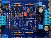
Photo of the wonky channel is attached. I will figure out how to do a diode mode test, and report back with what I find out.
Thanks.
Attachments
underside, pls
and try bigger resolution ........ every hair counts
Thanks, Zen. Photo of the underside attached. I think you need to open it in a separate tab, then you have the option of full glorious magnification. The photo is full size out of my iPhone XS, so I know it's big enough. I can't get it to fully magnify when I simply click the inline version. Am I missing a setting for image upload that allows full size access in the forum post when clicked?
Also, went back and measured every resistor on both channels. These were the ones with variances that were very noticeably different - compared channel to channel:
R1 - 36.4mV
R27 - 43.8 mV (ok, this ones not too different)
R2 - 36.6 mV
R28 - 0
R3 - 1.8mV
R40 - 490mV
R5 - 120mV
R37 - 24mV
R16 - .3mV
R43 - 10.34V
R17 - 0
R29 - 3.85V
Every other measurement between resistors channel-to-channel shows values that are the same or very close to. I gotta go read up on how to do a diode mode test. I appreciate everyone's help. Thanks again.
Attachments
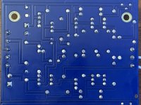
pic looks good - same as soldering, as far as I can see
now, end of not so long as of full day, so me better not to look at numbers you posted, now
if nobody chimes in, I will tomorrow
regarding diode test, skip that for later steps ( in your learning curve)
for now - use buzzer terst position(it beeps for everything under 30 to 50 ohms, depending on meter production) - that's tool for checking continuity
say -- one probe on tiny leg of JFet, other probe to resistor pin on same trace
if you hear buzz, JFet pin is (hopefully) properly soldered
good call - always use flux helper liquid, when soldering SMD parts
it's more helpful than Viagra
Try carefully reflowing your jfets. I had a similar problem on one of my builds and it turned out to be a bad joint on one of those little buggers.
Photo of the wonky channel is attached. I will figure out how to do a diode mode test, and report back with what I find out.
Thanks.
I’d do exactly as Choky and PJN prescribed. And focus my beep test to the cold-looking joints of Q21 and Q24. Reflow with liquid flux is preferred, as grease might make contact between legs if it gets under the transistor (tight space, difficult to clean). Careful when reflowing, they aren’t too happy with high temps and multiple reheats, imoe.
for now - use buzzer terst position(it beeps for everything under 30 to 50 ohms, depending on meter production) - that's tool for checking continuity
say -- one probe on tiny leg of JFet, other probe to resistor pin on same trace
if you hear buzz, JFet pin is (hopefully) properly soldered
Try carefully reflowing your jfets. I had a similar problem on one of my builds and it turned out to be a bad joint on one of those little buggers.
Checked the JFETs and the continuity was bad on Q21, which seems to make sense based on the issues I've been having. I will remove, clean and reflow that one and see if it fixes the problem. All of the others seem to be working properly. Thanks again for the guidance. I'll report back with results.
Last edited:
Hi, nice to see you got some results!
I’d be hesitant in removing the JFET. I recommend you just reflow for starters. They are easy to break, and hard to pull without destroying them.
Also, be careful with pliers close to the pcb if you choose to remove it. If you scratch the PCB, you could have issues with stability if copper gets in contact with for example flux residue etc.
A flux pen helps with reflow of SMD components (also initial installation):
https://amazon.com/gp/product/B07B53LNGX
https://amazon.com/gp/product/B07B53LNGX
Try carefully reflowing your jfets. I had a similar problem on one of my builds and it turned out to be a bad joint on one of those little buggers.
My first one cleared up once I scrubbed the tiny jfet pads with iso and tooth brush.
Russellc
I checked and reflowed the jfets which solved a number of issues. I can now adjust dc offset on the output of that channel via P1, and all but two of the resistor measurements between channels are the same. The only two that are still off are R40 and R43. Does that mean it's a Q21 issue, like maybe the jfet is bad? Good idea to replace and measure again?
Wait a minute for choky to respond. Once he had finished watching the re-run of Eurovision song contest.
Do you have replacements from the same reel? Else you could end up with different currents in your ccs.
Cheers,
Andy
Do you have replacements from the same reel? Else you could end up with different currents in your ccs.
Cheers,
Andy
Wait a minute for choky to respond.
Do you have replacements from the same reel? Else you could end up with different currents in your ccs.
Thanks, Andy. I have two more jfets from the same reel, so I should be good to replace one if needed. I'll wait and see what choky has to say.
Choky is short with time today (and tyoing from phone), so justnreplace them if you're confident
do not forget flux
do not forget flux
- Home
- Amplifiers
- Pass Labs
- Wayne's BA 2018 linestage