Bubba177 (or anyone else),
Here are some photos of my build, including the power supply.
I posted a few posts back (2999), hoping for some insight into a problem I'm having with my recent build - wondering if anyone has any idea what's gone wrong?
Any help appreciated!
point me to schematic having R27 and R28 in nomenclature (so being appropriate to pcb)
I only know of schm in post #1 and there are none of these
in short, if source resistors of JFets are not having same voltage across, JFet is suspicious, that side with no voltage
I know it's PITA to check and replace them , so check everything around and - if everything else is good - you (or Gremlins) conducted deadly soldering act
Hi 6L6,
Apologies for schematic confusion! I was using the numbering on the boards. The schematic numbers are R1 = 69.4mV, R2 = 0mV. That would make Q2 the dodgy JFet? I'll go ahead and swap it out.
Thanks for the help 🙂
Apologies for schematic confusion! I was using the numbering on the boards. The schematic numbers are R1 = 69.4mV, R2 = 0mV. That would make Q2 the dodgy JFet? I'll go ahead and swap it out.
Thanks for the help 🙂
Jfet replaced. DC offset stable.
Beautiful sounds! Mmmmmm...
Thanks Mikerodig27 and Zen Mod. Deadly soldering act undone.
I think that maybe on my first attempt I was too worried about making sure the SMDs were properly soldered to the board, thus cooked one. Following a suggestion from Andynor many posts back, I used a meter to check continuity from the SMD legs to their adjacent PC terminals, rather than trying to get a visual on whether or not the legs were soldered. Much more elegant (thanks Andynor).
And thanks Wayne Coulburn for the lovely design.
Happy listening ahead 🙂

Curse those gremlins.
We are the gremlins


BTW: that tip I wrote, like so much else, is from the Mighty’s head. Just passing his wisdom along 🙂
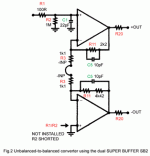
I have two of the DIY Audio 2018 boards. I’d like to run them as a single ended to balanced converters as shown in this Borbely version. The 6 db gain per stage is fine for my application. I’m planning to use the bigger Toshiba outputs.
Comments on how to select resistor values for the 2018 to set the gain on each stage are welcome.
From what I can figure out so far R11 would remain 27k4 , the series value of the 2 of R3 would total 27k4 (and maybe use just a single resistor) ,
R11 on the lower stage would be is a 5k ohm trimpot in series with a 52k3 to trim the gain, and the input resistors on the lower gain stage positive input are shorted.
Attachments
Last edited:
Actually using 2 of R3 ( total 27k4) and just run a jumper under the board between the 2 connections would mean no cutting
Elwood, I was thinking of doing something similar. What size is your chassis? Could you post some photos?
Thanks!
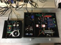
jazzman - The enclosure size is W 420mm X D 340mm X H 90mm. The UFSP took most of the room inside , the BA2018 boards are stacked on top of each other and the shunt regulators for the UFSP are mounted vertical. The remote power supply is for the UFSP.
Attachments
OMG, super cool. UFSP is a treat as well (also worth playing around with original FSP+SUTs, by comparison, if running MC carts).
What do you have going on there for switching? (and volume?) I have all the parts for another BA2018 build and feel obligated to set it up as dual-mono this time, maybe with VRDN, since I have one already built...so, planning phase...
What do you have going on there for switching? (and volume?) I have all the parts for another BA2018 build and feel obligated to set it up as dual-mono this time, maybe with VRDN, since I have one already built...so, planning phase...
Input switching and volume use relays, first project with a remote, controls on-off, input, volume, balance and mute.
Power supply for relay control and display also has 30A relay which turns on-off PS for BA2018.
Power supply for relay control and display also has 30A relay which turns on-off PS for BA2018.
Elwood makes my stuff look like some 1930’s crap. Not that it sounds bad. Elwood just took it all out on this preamp. Thanks for the inspiration! 🙂
Thanks guys,
I could not really see Q1 (actually it was Q22) because R27 was right in the way. Studying the schematic it seemed that Q22 or Q23 could be the problem. I removed R27 and was able to see that Q22's gate terminal looked suspicious. I just removed Q22, cleaned the area good and installed a spare 2SK209 and again cleaned with alcohol and a brush.
After reinstalling R27 I powered it up - things were better - no voltage across the input but DC offset on the problem channel was all over the place and fluctuating "oddly" - made me think it was a bad solder joint. I reflowed the other jfets and now it works great. Offset close to zero on both channels.
My attenuators should arrive Monday so I can test it out on my old system - a dual mono chip amp I built years ago and use in my home office/studio.
Again thanks for the help and moral support,
Ralph
- Home
- Amplifiers
- Pass Labs
- Wayne's BA 2018 linestage