It has been a while I blogged about this project.
Meanwhile I built revision three of the front end with some silly bugs fixed and implemented the differential cascodes.
I haven't powered this up yet.
Some side quests kept me busy like my day job drained all my energy for quite some time.
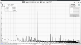
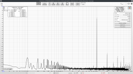
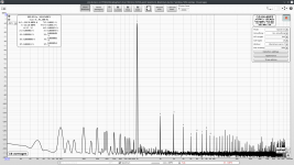
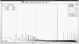
However, I'm currently doing measurements and thought I could share some pictures of the spectrum.
Current setup is with the revision two front end, revision two diamond driver stage and the 4x BJT output stage.
Main power supply voltage has doubled. Now I have +/-50V idle, which is a reasonable power supply voltage for domestic use I guess.
Note that I'm having issues with mains frequency noise and I believe this is because I changed the auxiliary power supplies to voltage doublers from the floating supplies I had before. I hope I will sort this out or revert back to the floating supplies where I had no such issues.
So just ignore the mains noise and its harmonics.
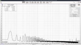
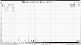
I present four measurements here:
1kHz and 10kHz with 8Vpp into 4 Ohm
1kHz and 10kHz with 80Vpp into 4 Ohm
I'm not used to perform such measurements and I might be doing something wrong.
I don't know whether the measurement result is something to be proud of.
What do you think?
Meanwhile I built revision three of the front end with some silly bugs fixed and implemented the differential cascodes.
I haven't powered this up yet.
Some side quests kept me busy like my day job drained all my energy for quite some time.
However, I'm currently doing measurements and thought I could share some pictures of the spectrum.
Current setup is with the revision two front end, revision two diamond driver stage and the 4x BJT output stage.
Main power supply voltage has doubled. Now I have +/-50V idle, which is a reasonable power supply voltage for domestic use I guess.
Note that I'm having issues with mains frequency noise and I believe this is because I changed the auxiliary power supplies to voltage doublers from the floating supplies I had before. I hope I will sort this out or revert back to the floating supplies where I had no such issues.
So just ignore the mains noise and its harmonics.
I present four measurements here:
1kHz and 10kHz with 8Vpp into 4 Ohm
1kHz and 10kHz with 80Vpp into 4 Ohm
I'm not used to perform such measurements and I might be doing something wrong.
I don't know whether the measurement result is something to be proud of.
What do you think?
Attachments
I believe the mains frequency noise issue is an inherent problem with the voltage doubler power supply and I likely won't be able to solve this.
This kind of power supply injects charging pulses into my sensitive ground and right now I cannot imagine how to prevent that easily.
I could add some linear regulators after the voltage doublers, return the charging pulses to somewhere else and this should work I guess. But then the voltage headroom gained would be gone mostly plus the cost and complexity is in the region of the floating supplies again or even higher.
What a shame because the idea of the voltage doublers is very appealing, especially because with my unusual transformer arrangement, the doubled voltage would not be twice the main power supply voltage, but 1.5x, means around 75V, which is a good middle ground.
However, even with the floating auxiliary power supplies, I still have some disturbance of the noise floor, although much lower.
Now this is entirely unrelated to mains frequency (50 Hz).
Any ideas what might be the root cause?
Attachments
Some notes regarding the main power supply and DC bias:
I use two 160VA todoids with two 18V secondaries each. They stem from my very first amplifier that I built as a teen so this is not really a deliberate design decision. However, this gives nice flexibility to wire the secondaries parallel or in series. Previously I had them parallel, now they are in series.
With only one channel connected and loaded by OPS bias current only, idle voltage is +/- 51V.
With one channel driving 80Vpp into a 4 Ohm load, the power supply sags to 45V.
I lose another 0.5V due to the 0.1 Ohm filter resistors that are part of the OPS.
OPS bias right after start up is 22mV across the 0.22R emitter resistors, thus 100mA.
After full load for a while, the radiator is soaked with energy and scalding hot (laying fins down on the table, thus no convection at all).
The driver stage radiator is oriented the wrong way, too, so also has not much convection.
When super hot, bias climbs to 28mV, thus 127mA.
This indicated that the whole arrangement has a positive temperature coefficient.
I guess that once the radiator is mounted to the chassis correctly, the effect is much less dramatic.
During measurements I experienced a funny phenomenon:
I could hear the test tones although the amp was driving a resistor load.
The sound seems to originate from the driver stage I believe.
First I thought the sound comes from the output stage, but I'm not that sure anymore.
In order to find the exact source, I would need to use a microphone for measuring.
What could be the components that emit sound?
This is what I have on the boards:
- Semiconductors (BJTs and diodes)
- Aluminum electrolytic capacitors
- Polyester film capacitors
- Polypropylene film capacitors
- C0G / NP0 ceramic capacitors
- X7R ceramic capacitors (only on the driver module and only for power supply bypassing)
Forget about the THD measurements posted earlier. I might be having an issue with my load and the amplifier might not have been loaded as intended.
I'm still optimizing the amplifier and just stumbles across something I can't explain:
Occasionally I experience some oscillation under some unusual conditions and tried to figure out what might cause this.
In simulation, there is a gain peak at ~15MHz and it seems that the current mirror degeneration seems to have an effect on this.
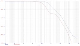
Here is the loopgain with different degeneration:

Gain peak with 200R degeneration.

Gone with 475R degeneration.
Does anybody have an idea why this happens?
I'm still optimizing the amplifier and just stumbles across something I can't explain:
Occasionally I experience some oscillation under some unusual conditions and tried to figure out what might cause this.
In simulation, there is a gain peak at ~15MHz and it seems that the current mirror degeneration seems to have an effect on this.
Here is the loopgain with different degeneration:
Gain peak with 200R degeneration.
Gone with 475R degeneration.
Does anybody have an idea why this happens?
Day 543.
I did not have an opportunity yet to test the increased degeneration of the current mirrors.
But I found out that I indeed damaged my dummy load resistor network. One of the 35W metal film resistors fused.
Thus, the posted spectrum plots are likely without any load, LOL!
Currently the amplifier is not working at all and the reason is that I removed all 100nF film caps for power supply decoupling.
The reason for the film cap removal is that I figured out that any low ESR capacitor will make the CFP capacitance multipliers go unstable. Thanks Peufeu for explaining. If you are interested in stabilizing CFPs, read CFP Complementary Feedback Pair - when and how to compensate for stability?
So until I have high ESR caps to use as local decoupling, the amplifier is not functional.
The effect I'm observing is that after power up, a DC offset slowly develops until it reaches almost the full power supply voltage.
I guess the reason is some oscillation, but not full bore, instead a very faint oscillation somewhere that apparently gets rectified somehow and builds up the DC offset.
Fascinating is that I can measure 25V across the (16V rated) 2x470uF caps of the feedback network. This should never happen because the maximum voltage at this node is the power supply rail voltage divided by the feedback network (gain=21). I installed the Zener protection diodes across those caps now.
Also some transistors are getting hot that absolutely should stay cool during normal operation.
This is a good example how a bad power distribution network can mess up any circuit.
While I'm waiting for parts to arrive, I did some measurements with the revision 2 front end (with TPC, but without new fancy bootstrap for the input LTP) and the output stage configured as diamond buffered triple.
This time I made sure that the dummy load of 8R really worked and got warm, but did not burn again.
Here are some numbers:
1kHz THD+N at 3V2pp into 8R: 0.016%
1kHz THD+N at 26Vpp into 8R: 0.0018%
1kHz THD+N at 36Vpp into 8R: 0.0013%
1kHz THD+N at 52Vpp into 8R: 0.00099%
1kHz THD+N at 78Vpp into 8R: 0.00075%
Which is kind of weird because why is THD getting better with higher level? I would expect the opposite.
CCIF 19/20kHz at 26Vpp into 8R: 0.0034%
CCIF 19/20kHz at 52Vpp into 8R: 0.0034%
Which also does not make much sense to me since I can see in the spectrum that the harmonics do grow a bit at higher signal level.
I believe I'm measuring nonsense. I know that I'm not good at measuring anything. Very likely the rising THD with lowering signal level is my measurement setup fault.
Does anybody know good literature how to properly measure audio performance metrics?
Here is a plot of THD vs level at high power, which seems to somewhat make sense to me:

This shows that distortion is dominated by second and third harmonics until roughly 1kHz. With rising frequency the third harmonic defines overall distortion.
This time I made sure that the dummy load of 8R really worked and got warm, but did not burn again.
Here are some numbers:
1kHz THD+N at 3V2pp into 8R: 0.016%
1kHz THD+N at 26Vpp into 8R: 0.0018%
1kHz THD+N at 36Vpp into 8R: 0.0013%
1kHz THD+N at 52Vpp into 8R: 0.00099%
1kHz THD+N at 78Vpp into 8R: 0.00075%
Which is kind of weird because why is THD getting better with higher level? I would expect the opposite.
CCIF 19/20kHz at 26Vpp into 8R: 0.0034%
CCIF 19/20kHz at 52Vpp into 8R: 0.0034%
Which also does not make much sense to me since I can see in the spectrum that the harmonics do grow a bit at higher signal level.
I believe I'm measuring nonsense. I know that I'm not good at measuring anything. Very likely the rising THD with lowering signal level is my measurement setup fault.
Does anybody know good literature how to properly measure audio performance metrics?
Here is a plot of THD vs level at high power, which seems to somewhat make sense to me:
This shows that distortion is dominated by second and third harmonics until roughly 1kHz. With rising frequency the third harmonic defines overall distortion.
Usually, it is normal for amplifier with ordinary Miller compensation and/or MIC compensation.Here are some numbers:
1kHz THD+N at 3V2pp into 8R: 0.016%
1kHz THD+N at 26Vpp into 8R: 0.0018%
1kHz THD+N at 36Vpp into 8R: 0.0013%
1kHz THD+N at 52Vpp into 8R: 0.00099%
1kHz THD+N at 78Vpp into 8R: 0.00075%
Which is kind of weird because why is THD getting better with higher level? I would expect the opposite.
If you use OITPC compensation from Dadod, you should get better THD at low level in simulation.
Meanwhile I figured out why THD+N at low signal level is higher: Because the SNR is worse.
Here is THD vs. level of my DAC fed right into my ADC:

For the most part, harmonics are buried in the noise floor, yet THD+N is abysmal due to poor SNR.
Also, setting REW to dBFS is misleading. With the plot set to dBc, it makes much more sense.
Here is THD vs. level of my DAC fed right into my ADC:
For the most part, harmonics are buried in the noise floor, yet THD+N is abysmal due to poor SNR.
Also, setting REW to dBFS is misleading. With the plot set to dBc, it makes much more sense.
I finished my fancy capacitors and installed them. However, I'm still facing the latch-up of the output to the positive power supply. Apparently I broke something.
And the reason some parts were damaged is that I left away the protection circuitry:
I have Zener Diodes across the large electrolytic capacitors (rated 16V) where I measured about 25V, but left the diodes away. Bad idea, but the caps apparently survived.
I also have the clipping circuitry at the amplifier inputs that would clip any voltage in excess of +/-5.4V to protect the LTP transistors. For the inverting input, this would be somewhat redundant because there are Zeners across the electrolytic caps already. Of course, the clipping circuitry was not installed either. The transistors are dead of course and I replaced them.
At this point I like to mention something that is important to keep in mind when using feedback baker clamps the way I do:
There is no attenuation of the signal going to the inverting input and there should be some clamps to protect the input by all means.
here is an illustration:

This means that in case the output latches to the supply rail, the supply rail will be at the inverting input.
I still need to figure out what exactly is broken and causes the DC offset in the first place.
Edit:
I forgot to mention that the transistor feeding the clipped signal back to the inverting input was also damaged due SOA violation. This is even more a problem if the inverting input is protected by a voltage clamp. I installed much more powerful transistors now (MJE340 / MJE350). Good is that I bias the second LTP with a CCS so current (and thus damage) is limited.
And the reason some parts were damaged is that I left away the protection circuitry:
I have Zener Diodes across the large electrolytic capacitors (rated 16V) where I measured about 25V, but left the diodes away. Bad idea, but the caps apparently survived.
I also have the clipping circuitry at the amplifier inputs that would clip any voltage in excess of +/-5.4V to protect the LTP transistors. For the inverting input, this would be somewhat redundant because there are Zeners across the electrolytic caps already. Of course, the clipping circuitry was not installed either. The transistors are dead of course and I replaced them.
At this point I like to mention something that is important to keep in mind when using feedback baker clamps the way I do:
There is no attenuation of the signal going to the inverting input and there should be some clamps to protect the input by all means.
here is an illustration:
This means that in case the output latches to the supply rail, the supply rail will be at the inverting input.
I still need to figure out what exactly is broken and causes the DC offset in the first place.
Edit:
I forgot to mention that the transistor feeding the clipped signal back to the inverting input was also damaged due SOA violation. This is even more a problem if the inverting input is protected by a voltage clamp. I installed much more powerful transistors now (MJE340 / MJE350). Good is that I bias the second LTP with a CCS so current (and thus damage) is limited.
Last edited:
I made up my mind what might have happened that lead to the sequential destruction of the front end and figured out some potential issues, which lead to an extensive redesign of many circuits. The CCS have changed and so has the current mirror. Also the power supply reference voltage generation was updated and I got rid of the capacitance multipliers. Bob's amp has excellent PSRR so they are superfluous anyway.
During the course of redesigning the module I conducted a more detailed investigation of the current mirror related gain peak phenomenon. I find this very surprising and interesting and like to share my ideas and results with you.
In post #65 I presented my findings about the current mirror degeneration resistors affecting the gain peak at ~18MHz. I changed the current mirror from an emitter follower enhanced to a Wilson mirror just to observe the gain peak again. Even a very basic current mirror shows such a gain peak. Such gain peaks are a sure sign of instability that will occur sporadically under some operating conditions.
This for example is the gain peak with a simple current mirror:

Investigating the current mirror on its own shows that there is nothing wrong with the current mirror and there is no gain peak at all.
Since the fourth revision of this amplifier front end is going to use a Wilson current mirror, I tried several things to get rid of the peak with this kind of current mirror.
Here is one attempt using a base resistor with either one Ohm or 1k Ohm to illustrate the effect:


Clearly the resistor suppresses the gain peak and exaggerating the effect by increasing the resistance shows that some phase anomalies are associated with removal of the gain peak:

Investigating the current mirror in isolation shows that addition of this resistor actually causes a gain peak at the current mirror output:

Without resistor, there is some roll-off and increasing the resistor extends the bandwidth into peaking at the cost of huge phase shift.
So it appears that one gain peak nulls the other.
The same effect can be observed with a capacitor in the current mirror instead:

The loopgain plot looks almost the same, thus is omitted.
At this point I wondered why current mirrors with such peaky response fix another peak and what might be the root cause. The current mirror is part of the VAS output and loaded by a R-C-snubber to ground. This is aiding stability and often recommended. Also, the VAS output appears less inductive (a bit more more capacitive) to the output stage, which helps with maintaining stability of the output stage. Thus, the snubber is good practice in any case.
But the snubber rolls off the current mirror output and this seems to cause the gain peak: With the snubber removed, there is no gain peak anymore.
Here is how the current mirror output looks like with the snubber capacitor stepped:

So the peaking of the mirror output is partially compensating for the current mirror output roll-off caused by the snubber load.
Somehow the roll-off at the CM output by the snubber causes this gain peak. The mechanism of this effect is not clear to me however.
Here I set the snubber cap to 100pF and stepped the capacitor inside the current mirror:

The response of the current mirror is somewhat restored, although the solution looks like a band aid. To generate a peak just to get rid of it again using a snubber appears stupid to me.
Any ideas anyone?
Many guys here designed amplifiers with this topology and might have made similar observations already.
During the course of redesigning the module I conducted a more detailed investigation of the current mirror related gain peak phenomenon. I find this very surprising and interesting and like to share my ideas and results with you.
In post #65 I presented my findings about the current mirror degeneration resistors affecting the gain peak at ~18MHz. I changed the current mirror from an emitter follower enhanced to a Wilson mirror just to observe the gain peak again. Even a very basic current mirror shows such a gain peak. Such gain peaks are a sure sign of instability that will occur sporadically under some operating conditions.
This for example is the gain peak with a simple current mirror:
Investigating the current mirror on its own shows that there is nothing wrong with the current mirror and there is no gain peak at all.
Since the fourth revision of this amplifier front end is going to use a Wilson current mirror, I tried several things to get rid of the peak with this kind of current mirror.
Here is one attempt using a base resistor with either one Ohm or 1k Ohm to illustrate the effect:
Clearly the resistor suppresses the gain peak and exaggerating the effect by increasing the resistance shows that some phase anomalies are associated with removal of the gain peak:
Investigating the current mirror in isolation shows that addition of this resistor actually causes a gain peak at the current mirror output:
Without resistor, there is some roll-off and increasing the resistor extends the bandwidth into peaking at the cost of huge phase shift.
So it appears that one gain peak nulls the other.
The same effect can be observed with a capacitor in the current mirror instead:
The loopgain plot looks almost the same, thus is omitted.
At this point I wondered why current mirrors with such peaky response fix another peak and what might be the root cause. The current mirror is part of the VAS output and loaded by a R-C-snubber to ground. This is aiding stability and often recommended. Also, the VAS output appears less inductive (a bit more more capacitive) to the output stage, which helps with maintaining stability of the output stage. Thus, the snubber is good practice in any case.
But the snubber rolls off the current mirror output and this seems to cause the gain peak: With the snubber removed, there is no gain peak anymore.
Here is how the current mirror output looks like with the snubber capacitor stepped:
So the peaking of the mirror output is partially compensating for the current mirror output roll-off caused by the snubber load.
Somehow the roll-off at the CM output by the snubber causes this gain peak. The mechanism of this effect is not clear to me however.
Here I set the snubber cap to 100pF and stepped the capacitor inside the current mirror:
The response of the current mirror is somewhat restored, although the solution looks like a band aid. To generate a peak just to get rid of it again using a snubber appears stupid to me.
Any ideas anyone?
Many guys here designed amplifiers with this topology and might have made similar observations already.
Hi
Your gain phase plots look weird to me. Also better chose different color in the plot ...
To my understanding it should look like in the ac analysis posted below.
At zero gain your phase should be around + 45 degrees.
At zero degrees phase, the gain should be down to -10dB or more.
No peaks... Peak in the gain plot before falloff means overshoot on square waves.
Standard gain is 28dB.
Please somebody correct me if I´m wrong.
Attachments
As you noticed yourself, you started very big.
However, every additional amp stage or additional feature makes it more difficult to compensate the whole thing.
If you start simple, step by step, it is more easy.
I tried the LTP cascode connection via external transistor but it did not give any improvement in thd in simulation.
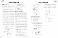
It is in the Kenwood L-A1 service manual. They rave about the improvement.
However, every additional amp stage or additional feature makes it more difficult to compensate the whole thing.
If you start simple, step by step, it is more easy.
I tried the LTP cascode connection via external transistor but it did not give any improvement in thd in simulation.
It is in the Kenwood L-A1 service manual. They rave about the improvement.
You’re right this can’t be stable and it turned out it isn’t. Just a brain fart, sorry. I should have verified this more thoroughly.
I experimented with more stupid mods to the current mirror like capacitors parallel to the degeneration resistors (not good) or inductors in series (could maybe work, but no).
Degeneration of the mirror has dramatic effect on the gain peak, but there is no clear trend like more is better.
Latest finding is that an unusal mod of the Wilson mirror produces good results in both AC and transient simulation. The image attached shows what I mean. Unfortunately I forgot the context where I have it from.

The circuit on the right seems a worthwhile modification to the full Wilson mirror. This can be implemented using two transistors instead of the dual emitter one that only exists in ICs. Whether this still works well with sample to sample variations of discrete transistors is another story.
Of course I have no idea why this works well, but I plan to figure it out.
The loopgain looks weird due to dual pole compensation BTW. I found TPC easier to get right than MIC of the original design, but this might be having to do with enclosing an unstable output stage into the feedback loop back when I experimented with MIC. Maybe I give MIC another try. If everything fails, plain Miller is an option.
Yes, I started way too big. Reading textbooks makes it seem too easy getting ideas to work well, but in fact there are countless pitfalls lurking behind every great idea.
Thanks for mentioning the service manual. I’m going to have a closer look at this.
I experimented with more stupid mods to the current mirror like capacitors parallel to the degeneration resistors (not good) or inductors in series (could maybe work, but no).
Degeneration of the mirror has dramatic effect on the gain peak, but there is no clear trend like more is better.
Latest finding is that an unusal mod of the Wilson mirror produces good results in both AC and transient simulation. The image attached shows what I mean. Unfortunately I forgot the context where I have it from.
The circuit on the right seems a worthwhile modification to the full Wilson mirror. This can be implemented using two transistors instead of the dual emitter one that only exists in ICs. Whether this still works well with sample to sample variations of discrete transistors is another story.
Of course I have no idea why this works well, but I plan to figure it out.
The loopgain looks weird due to dual pole compensation BTW. I found TPC easier to get right than MIC of the original design, but this might be having to do with enclosing an unstable output stage into the feedback loop back when I experimented with MIC. Maybe I give MIC another try. If everything fails, plain Miller is an option.
Yes, I started way too big. Reading textbooks makes it seem too easy getting ideas to work well, but in fact there are countless pitfalls lurking behind every great idea.
Thanks for mentioning the service manual. I’m going to have a closer look at this.
Active Cascode Current Mirror / Cascode Current Mirror With Super Beta Helper


Attachments
-
Active Cascode Current Mirror.pdf528.6 KB · Views: 122
-
Active Cascode Topology.pdf1 MB · Views: 116
-
Analysis simulation and circuit implementation.pdf511.3 KB · Views: 98
-
Cascode current mirror circuit.pdf640 KB · Views: 106
-
Cascode Current Mirror With Super Beta Helper.pdf346.6 KB · Views: 110
-
M12-DRV.pdf43.3 KB · Views: 104
-
M12-OUT.pdf36.9 KB · Views: 109
-
Precision current mirror arrays.pdf1,023.1 KB · Views: 107
Thanks for all the inspiration.Active Cascode Current Mirror / Cascode Current Mirror With Super Beta Helper
View attachment 1113314
View attachment 1113315
View attachment 1113316
View attachment 1113318
View attachment 1113320
View attachment 1113319
View attachment 1113317
View attachment 1113321
View attachment 1113322
View attachment 1113323
View attachment 1113324
View attachment 1113325
I tried a few better mirrors against the basic two transistor mirror in the input diff amp but the simulation did not show any improvements so far.
Thanks for pointing me to the Kenwood service manual. Interesting to see an actual implementation of the concept that went into mass production. However, after reading this I'm left a bit confused:
In figure #1 they show a very basic bootstrapping scheme and point of the two shortcomings of this circuit: The CCS does not have a cascode thus Cob of Q5 worsens performance of the CCS significantly as pointed out in the manual. Also, they point out how poor R5 performs as constant current source and how this ruins the circuit.
Both shortcomings are addressed in figure #3 (simplification of figure #2) with the unnecessary complication of adding an emitter follower to drive the cascode offset. They explain that not dumping the constant current flowing through D1 (fig. #2) into the tail node reduces noise, but I doubt that this is a serious concern. I don't see anything wrong with connecting this together like in figure #1. According to my experience so far, this is a simple low risk way of bootstrapping that is good enough.
What actually confuses me is figure #2. I don't know where to start explaining what is confusing since a lot of things in the figure #2 schematic do not make much sense to me. I believe this is over-complicated adding risk with little benefit and the main purpose is generating a USP for marketing.
The next revision of my front end will feature two options for bootstrapping the cascodes:
One with with two individual emitter follower buffers attached to the emitters. This is the option colored in orange.
The other is dumping the current of the diodes generating the offset into the LTP emitter degeneration resistors. This is the green option (active / Hawksford cascode).
In order to keep this stable, I added capacitors parallel to the diodes. I have seen such capacitors in many schematics including the ones Levinson Mark posted and this may help to shunt the diodes at high frequency reducing the bootstrapping. It just seems the capacitors would need to have much larger value.

There is a more detailed discussion about various bootstrapping schemes for the LTP here:
https://www.diyaudio.com/community/threads/driven-cascode-novelty-circuit.389449/
Bernhard: I agree that a gain of 28dB makes much more sense and plan to increase gain accordingly. Thanks for mentioning!
Regarding the current mirrors:
I found out where I have the schematic of the Wilson mirror with dual emitter transistor from: Wilson Current Mirror
The caption reads: Figure 4a) Four transistor Wilson current mirror (note: schematic on the left); 4b) Variant that removes peak in high-frequency response (note: schematic on the right).
HF stabilization by addition of the fifth transistor seems to work indeed. I played a bit with this arrangement and found that the fifth transistor does not even need to be matched: It even works well with a different model assigned.
Different mirrors behave very different, but in most amplifiers this does not really matter too much.
Some mirrors are more linear and stable than others and while linearity may not seem to matter in amplifiers with a lot of global negative feedback, I experienced issues with stability.
This gain peak is haunting me from the beginning on and until now I thought it has to do with compensation, which is only partially true.
Linearity of the mirrors matters most in applications without tons of NFB to straighten out crooked circuits performance (just like the Krell buffers posted by Levinson Mark. I haven't simulated the buffers (yet), but I bet they show impressively low distortion even without a feedback loop. The Boxall cascode is prone to instability however.
I found a current mirror comparison simulation file here on the forum some time ago and expanded it a bit with more variants.
The result is quite interesting.
For example THD at 20kHz of the mirrors in the simulation attached:
0.019% basic mirror
0.014% basic mirror with Boxall cascode
0.009% beta enhanced
0.0014% beta enhanced with cascode
0.0044% beta enhanced with Boxall cascode
0.0029% super beta enhanced
0.0015% super beta enhanced with cascode
0.0039% four transistor Wilson
0.0013% four transistor Wilson with cascode
0.004% five transistor Wilson
0.0017% five transistor Wilson with cascode
Also, the different mirrors show different HF response, some have wider bandwidth than others; some show peaking.
I attached the Spice file I got from the forum and extended for anybody interested playing around with some mirrors.
Levinson Mark: Thanks for all the inspiration, highly appreciated!
I did not know the super beta enhanced mirror yet.
And the correction stage is very unusual, never seen it before.
The active cascode is an interesting implementation of bootstrapping the Hawksford style. Great to see some examples how to do this.
Where do you have the input stage / correction stage / power stage schematics from?
The input stage design has a lot in similar with mine.
One of the main objectives of this front end is to make everything as linear as possible in order to lower higher order harmonics. At high frequency, say 20kHz, negative feedback is no longer that effective to reduce distortion.
With the gain set to 25dB, 500kHz UGLF Miller compensation, I would have gain = OLG at 20kHz. With two pole compensation, I still have ~15dB left over for reducing distortion. Now with 28dB gain, the situation looks a bit worse. This is the reason I first settled for lower gain and later went to TPC.
I plan to test the limits of compensation again and hope to settle at ~700kHz UGLF with TPC maybe. Lowering UGLF was related to exposing and getting rid of the gain peak that otherwise may easily get swamped. Means it is still there and causing trouble, but no longer clearly shows in the loopgain plot.
First part of eliminating the gain peak was to get the driver and output stage as a whole stable. This has helped a lot. Second part likely is the current mirror then.
In figure #1 they show a very basic bootstrapping scheme and point of the two shortcomings of this circuit: The CCS does not have a cascode thus Cob of Q5 worsens performance of the CCS significantly as pointed out in the manual. Also, they point out how poor R5 performs as constant current source and how this ruins the circuit.
Both shortcomings are addressed in figure #3 (simplification of figure #2) with the unnecessary complication of adding an emitter follower to drive the cascode offset. They explain that not dumping the constant current flowing through D1 (fig. #2) into the tail node reduces noise, but I doubt that this is a serious concern. I don't see anything wrong with connecting this together like in figure #1. According to my experience so far, this is a simple low risk way of bootstrapping that is good enough.
What actually confuses me is figure #2. I don't know where to start explaining what is confusing since a lot of things in the figure #2 schematic do not make much sense to me. I believe this is over-complicated adding risk with little benefit and the main purpose is generating a USP for marketing.
The next revision of my front end will feature two options for bootstrapping the cascodes:
One with with two individual emitter follower buffers attached to the emitters. This is the option colored in orange.
The other is dumping the current of the diodes generating the offset into the LTP emitter degeneration resistors. This is the green option (active / Hawksford cascode).
In order to keep this stable, I added capacitors parallel to the diodes. I have seen such capacitors in many schematics including the ones Levinson Mark posted and this may help to shunt the diodes at high frequency reducing the bootstrapping. It just seems the capacitors would need to have much larger value.
There is a more detailed discussion about various bootstrapping schemes for the LTP here:
https://www.diyaudio.com/community/threads/driven-cascode-novelty-circuit.389449/
Bernhard: I agree that a gain of 28dB makes much more sense and plan to increase gain accordingly. Thanks for mentioning!
Regarding the current mirrors:
I found out where I have the schematic of the Wilson mirror with dual emitter transistor from: Wilson Current Mirror
The caption reads: Figure 4a) Four transistor Wilson current mirror (note: schematic on the left); 4b) Variant that removes peak in high-frequency response (note: schematic on the right).
HF stabilization by addition of the fifth transistor seems to work indeed. I played a bit with this arrangement and found that the fifth transistor does not even need to be matched: It even works well with a different model assigned.
Different mirrors behave very different, but in most amplifiers this does not really matter too much.
Some mirrors are more linear and stable than others and while linearity may not seem to matter in amplifiers with a lot of global negative feedback, I experienced issues with stability.
This gain peak is haunting me from the beginning on and until now I thought it has to do with compensation, which is only partially true.
Linearity of the mirrors matters most in applications without tons of NFB to straighten out crooked circuits performance (just like the Krell buffers posted by Levinson Mark. I haven't simulated the buffers (yet), but I bet they show impressively low distortion even without a feedback loop. The Boxall cascode is prone to instability however.
I found a current mirror comparison simulation file here on the forum some time ago and expanded it a bit with more variants.
The result is quite interesting.
For example THD at 20kHz of the mirrors in the simulation attached:
0.019% basic mirror
0.014% basic mirror with Boxall cascode
0.009% beta enhanced
0.0014% beta enhanced with cascode
0.0044% beta enhanced with Boxall cascode
0.0029% super beta enhanced
0.0015% super beta enhanced with cascode
0.0039% four transistor Wilson
0.0013% four transistor Wilson with cascode
0.004% five transistor Wilson
0.0017% five transistor Wilson with cascode
Also, the different mirrors show different HF response, some have wider bandwidth than others; some show peaking.
I attached the Spice file I got from the forum and extended for anybody interested playing around with some mirrors.
Levinson Mark: Thanks for all the inspiration, highly appreciated!
I did not know the super beta enhanced mirror yet.
And the correction stage is very unusual, never seen it before.
The active cascode is an interesting implementation of bootstrapping the Hawksford style. Great to see some examples how to do this.
Where do you have the input stage / correction stage / power stage schematics from?
The input stage design has a lot in similar with mine.
One of the main objectives of this front end is to make everything as linear as possible in order to lower higher order harmonics. At high frequency, say 20kHz, negative feedback is no longer that effective to reduce distortion.
With the gain set to 25dB, 500kHz UGLF Miller compensation, I would have gain = OLG at 20kHz. With two pole compensation, I still have ~15dB left over for reducing distortion. Now with 28dB gain, the situation looks a bit worse. This is the reason I first settled for lower gain and later went to TPC.
I plan to test the limits of compensation again and hope to settle at ~700kHz UGLF with TPC maybe. Lowering UGLF was related to exposing and getting rid of the gain peak that otherwise may easily get swamped. Means it is still there and causing trouble, but no longer clearly shows in the loopgain plot.
First part of eliminating the gain peak was to get the driver and output stage as a whole stable. This has helped a lot. Second part likely is the current mirror then.
Attachments
Thanks for pointing me to the Kenwood service manual. Interesting to see an actual implementation of the concept that went into mass production. However, after reading this I'm left a bit confused:
In figure #1 they show a very basic bootstrapping scheme and point of the two shortcomings of this circuit: The CCS does not have a cascode thus Cob of Q5 worsens performance of the CCS significantly as pointed out in the manual. Also, they point out how poor R5 performs as constant current source and how this ruins the circuit.
Both shortcomings are addressed in figure #3 (simplification of figure #2) with the unnecessary complication of adding an emitter follower to drive the cascode offset. They explain that not dumping the constant current flowing through D1 (fig. #2) into the tail node reduces noise, but I doubt that this is a serious concern. I don't see anything wrong with connecting this together like in figure #1. According to my experience so far, this is a simple low risk way of bootstrapping that is good enough.
What actually confuses me is figure #2. I don't know where to start explaining what is confusing since a lot of things in the figure #2 schematic do not make much sense to me. I believe this is over-complicated adding risk with little benefit and the main purpose is generating a USP for marketing.
The next revision of my front end will feature two options for bootstrapping the cascodes:
One with with two individual emitter follower buffers attached to the emitters. This is the option colored in orange.
The other is dumping the current of the diodes generating the offset into the LTP emitter degeneration resistors. This is the green option (active / Hawksford cascode).
In order to keep this stable, I added capacitors parallel to the diodes. I have seen such capacitors in many schematics including the ones Levinson Mark posted and this may help to shunt the diodes at high frequency reducing the bootstrapping. It just seems the capacitors would need to have much larger value.
View attachment 1114708
There is a more detailed discussion about various bootstrapping schemes for the LTP here:
https://www.diyaudio.com/community/threads/driven-cascode-novelty-circuit.389449/
Bernhard: I agree that a gain of 28dB makes much more sense and plan to increase gain accordingly. Thanks for mentioning!
Regarding the current mirrors:
I found out where I have the schematic of the Wilson mirror with dual emitter transistor from: Wilson Current Mirror
The caption reads: Figure 4a) Four transistor Wilson current mirror (note: schematic on the left); 4b) Variant that removes peak in high-frequency response (note: schematic on the right).
HF stabilization by addition of the fifth transistor seems to work indeed. I played a bit with this arrangement and found that the fifth transistor does not even need to be matched: It even works well with a different model assigned.
Different mirrors behave very different, but in most amplifiers this does not really matter too much.
Some mirrors are more linear and stable than others and while linearity may not seem to matter in amplifiers with a lot of global negative feedback, I experienced issues with stability.
This gain peak is haunting me from the beginning on and until now I thought it has to do with compensation, which is only partially true.
Linearity of the mirrors matters most in applications without tons of NFB to straighten out crooked circuits performance (just like the Krell buffers posted by Levinson Mark. I haven't simulated the buffers (yet), but I bet they show impressively low distortion even without a feedback loop. The Boxall cascode is prone to instability however.
I found a current mirror comparison simulation file here on the forum some time ago and expanded it a bit with more variants.
The result is quite interesting.
For example THD at 20kHz of the mirrors in the simulation attached:
0.019% basic mirror
0.014% basic mirror with Boxall cascode
0.009% beta enhanced
0.0014% beta enhanced with cascode
0.0044% beta enhanced with Boxall cascode
0.0029% super beta enhanced
0.0015% super beta enhanced with cascode
0.0039% four transistor Wilson
0.0013% four transistor Wilson with cascode
0.004% five transistor Wilson
0.0017% five transistor Wilson with cascode
Also, the different mirrors show different HF response, some have wider bandwidth than others; some show peaking.
I attached the Spice file I got from the forum and extended for anybody interested playing around with some mirrors.
Levinson Mark: Thanks for all the inspiration, highly appreciated!
I did not know the super beta enhanced mirror yet.
And the correction stage is very unusual, never seen it before.
The active cascode is an interesting implementation of bootstrapping the Hawksford style. Great to see some examples how to do this.
Where do you have the input stage / correction stage / power stage schematics from?
The input stage design has a lot in similar with mine.
One of the main objectives of this front end is to make everything as linear as possible in order to lower higher order harmonics. At high frequency, say 20kHz, negative feedback is no longer that effective to reduce distortion.
With the gain set to 25dB, 500kHz UGLF Miller compensation, I would have gain = OLG at 20kHz. With two pole compensation, I still have ~15dB left over for reducing distortion. Now with 28dB gain, the situation looks a bit worse. This is the reason I first settled for lower gain and later went to TPC.
I plan to test the limits of compensation again and hope to settle at ~700kHz UGLF with TPC maybe. Lowering UGLF was related to exposing and getting rid of the gain peak that otherwise may easily get swamped. Means it is still there and causing trouble, but no longer clearly shows in the loopgain plot.
First part of eliminating the gain peak was to get the driver and output stage as a whole stable. This has helped a lot. Second part likely is the current mirror then.
The schematic diagram of input stage/correction stage/power stage comes from here:
http://diy.ucborgmann.de/index.php/...ekte/power-amp-mh-p100/schaltplaene?showall=1
http://diy.ucborgmann.de/images/PowerAmpMPH100/InputStage.png
http://diy.ucborgmann.de/images/PowerAmpMPH100/CorrectionStage.png
http://diy.ucborgmann.de/images/PowerAmpMPH100/PowerStage.png
http://diy.ucborgmann.de/images/PowerAmpMPH100/VRegP1.png

Did you simulate THD at 1 kHz ?Thanks for pointing me to the Kenwood service manual. Interesting to see an actual implementation of the concept that went into mass production. However, after reading this I'm left a bit confused:
In figure #1 they show a very basic bootstrapping scheme and point of the two shortcomings of this circuit: The CCS does not have a cascode thus Cob of Q5 worsens performance of the CCS significantly as pointed out in the manual. Also, they point out how poor R5 performs as constant current source and how this ruins the circuit.
Both shortcomings are addressed in figure #3 (simplification of figure #2) with the unnecessary complication of adding an emitter follower to drive the cascode offset. They explain that not dumping the constant current flowing through D1 (fig. #2) into the tail node reduces noise, but I doubt that this is a serious concern. I don't see anything wrong with connecting this together like in figure #1. According to my experience so far, this is a simple low risk way of bootstrapping that is good enough.
What actually confuses me is figure #2. I don't know where to start explaining what is confusing since a lot of things in the figure #2 schematic do not make much sense to me. I believe this is over-complicated adding risk with little benefit and the main purpose is generating a USP for marketing.
The next revision of my front end will feature two options for bootstrapping the cascodes:
One with with two individual emitter follower buffers attached to the emitters. This is the option colored in orange.
The other is dumping the current of the diodes generating the offset into the LTP emitter degeneration resistors. This is the green option (active / Hawksford cascode).
In order to keep this stable, I added capacitors parallel to the diodes. I have seen such capacitors in many schematics including the ones Levinson Mark posted and this may help to shunt the diodes at high frequency reducing the bootstrapping. It just seems the capacitors would need to have much larger value.
View attachment 1114708
There is a more detailed discussion about various bootstrapping schemes for the LTP here:
https://www.diyaudio.com/community/threads/driven-cascode-novelty-circuit.389449/
Bernhard: I agree that a gain of 28dB makes much more sense and plan to increase gain accordingly. Thanks for mentioning!
Regarding the current mirrors:
I found out where I have the schematic of the Wilson mirror with dual emitter transistor from: Wilson Current Mirror
The caption reads: Figure 4a) Four transistor Wilson current mirror (note: schematic on the left); 4b) Variant that removes peak in high-frequency response (note: schematic on the right).
HF stabilization by addition of the fifth transistor seems to work indeed. I played a bit with this arrangement and found that the fifth transistor does not even need to be matched: It even works well with a different model assigned.
Different mirrors behave very different, but in most amplifiers this does not really matter too much.
Some mirrors are more linear and stable than others and while linearity may not seem to matter in amplifiers with a lot of global negative feedback, I experienced issues with stability.
This gain peak is haunting me from the beginning on and until now I thought it has to do with compensation, which is only partially true.
Linearity of the mirrors matters most in applications without tons of NFB to straighten out crooked circuits performance (just like the Krell buffers posted by Levinson Mark. I haven't simulated the buffers (yet), but I bet they show impressively low distortion even without a feedback loop. The Boxall cascode is prone to instability however.
I found a current mirror comparison simulation file here on the forum some time ago and expanded it a bit with more variants.
The result is quite interesting.
For example THD at 20kHz of the mirrors in the simulation attached:
0.019% basic mirror
0.014% basic mirror with Boxall cascode
0.009% beta enhanced
0.0014% beta enhanced with cascode
0.0044% beta enhanced with Boxall cascode
0.0029% super beta enhanced
0.0015% super beta enhanced with cascode
0.0039% four transistor Wilson
0.0013% four transistor Wilson with cascode
0.004% five transistor Wilson
0.0017% five transistor Wilson with cascode
Also, the different mirrors show different HF response, some have wider bandwidth than others; some show peaking.
I attached the Spice file I got from the forum and extended for anybody interested playing around with some mirrors.
Levinson Mark: Thanks for all the inspiration, highly appreciated!
I did not know the super beta enhanced mirror yet.
And the correction stage is very unusual, never seen it before.
The active cascode is an interesting implementation of bootstrapping the Hawksford style. Great to see some examples how to do this.
Where do you have the input stage / correction stage / power stage schematics from?
The input stage design has a lot in similar with mine.
One of the main objectives of this front end is to make everything as linear as possible in order to lower higher order harmonics. At high frequency, say 20kHz, negative feedback is no longer that effective to reduce distortion.
With the gain set to 25dB, 500kHz UGLF Miller compensation, I would have gain = OLG at 20kHz. With two pole compensation, I still have ~15dB left over for reducing distortion. Now with 28dB gain, the situation looks a bit worse. This is the reason I first settled for lower gain and later went to TPC.
I plan to test the limits of compensation again and hope to settle at ~700kHz UGLF with TPC maybe. Lowering UGLF was related to exposing and getting rid of the gain peak that otherwise may easily get swamped. Means it is still there and causing trouble, but no longer clearly shows in the loopgain plot.
First part of eliminating the gain peak was to get the driver and output stage as a whole stable. This has helped a lot. Second part likely is the current mirror then.
You mean the Kenwood circuit?Did you simulate THD at 1 kHz ?
No, I haven't simulated it, but simulation would surely help to better understand it.
- Home
- Amplifiers
- Solid State
- VFA front end - the Bunnyphant