Short Christmas update while the tree is being decorated:
Since the setup with the folded driver runs more or less stable, I tried to figure out what is wrong with the DBT configuration.
When increasing the compensation, the amp is stable and also recovers from deliberate destabilization immediately.
Seems like the issue is related to compensation.
I'm just disappointed that UGLF is around 250kHz then.
With TPC, there is still a lot of NFB at 20kHz, but I don't want to believe that this is really the way to go.
Many years ago I built an amp with 10 pairs of HexFETs as OPS configured as simple dual EF and the amp had 500kHz UGLF and it seemed stable.
This is my first approach with a BJT OPS.
Are BJT OPS really that difficult to deal with?
Apart from the folded driver forming a dual EF, which is inherently more stable than a triple, the OPS is run in class A with the folded driver.
The OPS BJTs have roughly 20MHz fT at 100mA Ic and 40MHz fT at 1A Ic.
Maybe this is also a contributor to the stability.
I likely will experiment with running the DBT in class A to find out.
Getting back to simulation I found that the sim setup was off and once I corrected this, I saw the gain peak again.
This gain peak can easily get masked by high UGLF of the compensation loop and the amp looks stable then, but isn't.
The gain peak can be controlled by C3 and C4 of the diamond driver module. Maybe there are other ways to do this?
Increasing the capacitance lowers the gain peak and therefore increases phase margin at -180°.
Downside is that more capacitive loading of the previous EF destabilizes this stage then and also cuts into phase margin above ULGF.
This is why I have R5 and R6 to mitigate the load a bit, but too high resistance makes the capacitance ineffective again.
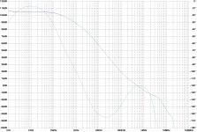
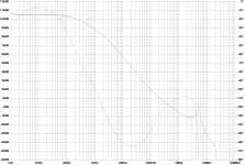
I increased C3 and C4 from 680pf to 1n5, but this didn't help with stability.
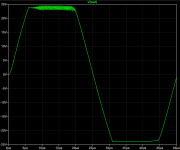
Attached two plots illustration the gain peak. The comparison is between 330pF (instead of 470pf) and 1n5 to illustrate the effect.
I guess I need to work at the compensation and learn more about TPC and how to apply this correctly.
Since the setup with the folded driver runs more or less stable, I tried to figure out what is wrong with the DBT configuration.
When increasing the compensation, the amp is stable and also recovers from deliberate destabilization immediately.
Seems like the issue is related to compensation.
I'm just disappointed that UGLF is around 250kHz then.
With TPC, there is still a lot of NFB at 20kHz, but I don't want to believe that this is really the way to go.
Many years ago I built an amp with 10 pairs of HexFETs as OPS configured as simple dual EF and the amp had 500kHz UGLF and it seemed stable.
This is my first approach with a BJT OPS.
Are BJT OPS really that difficult to deal with?
Apart from the folded driver forming a dual EF, which is inherently more stable than a triple, the OPS is run in class A with the folded driver.
The OPS BJTs have roughly 20MHz fT at 100mA Ic and 40MHz fT at 1A Ic.
Maybe this is also a contributor to the stability.
I likely will experiment with running the DBT in class A to find out.
Getting back to simulation I found that the sim setup was off and once I corrected this, I saw the gain peak again.
This gain peak can easily get masked by high UGLF of the compensation loop and the amp looks stable then, but isn't.
The gain peak can be controlled by C3 and C4 of the diamond driver module. Maybe there are other ways to do this?
Increasing the capacitance lowers the gain peak and therefore increases phase margin at -180°.
Downside is that more capacitive loading of the previous EF destabilizes this stage then and also cuts into phase margin above ULGF.
This is why I have R5 and R6 to mitigate the load a bit, but too high resistance makes the capacitance ineffective again.
I increased C3 and C4 from 680pf to 1n5, but this didn't help with stability.
Attached two plots illustration the gain peak. The comparison is between 330pF (instead of 470pf) and 1n5 to illustrate the effect.
I guess I need to work at the compensation and learn more about TPC and how to apply this correctly.
Attachments
This won't help your stability problem because it's a low-frequency thing, but an observation about your "BTC" capacitor. A tiny capacitor there has an outsized effect. If you look in my HPA thread, on the simulation, just putting a Baker clamp diode across the TPC network is enough to radically alter the compensation curve. It looks like you're splitting the low-frequency TPC poles (there's a break around 100Hz, then at about 2kHz). If you read the bottom of Harry Dymond's paper, he talks about adding a capacitor in series with the TPC resistor, which he incorrectly calls (and corrects in a revision) three-pole compensation. This capacitor nicely knocks down the TPC peak and it's a large value (around 150nF, IIRC) so may be less fiddly. Seems to work very nicely on simulation. Again, this probably won't fix your amplifier, but it's a nice technique to learn about, I think.
This may or may not be a helpful suggestion, but in the world of software development there's something called "thrashing" (not to be confused with other uses of the same term). It's when you have a really complicated program and you don't know why it's failing. You keep changing things without understanding the root cause, and you end up fixing one problem but causing others. When this happens to me, I will sometimes try to find the simplest possible implementation that works, then add features back in until it breaks. I know you're being very methodical so I apologize if I'm insulting you by stating the obvious.
In any case, if you get too frustrated, it might help to build a simpler model amplifier with fewer moving parts to give you more confidence and a better handle on these different compensation schemes. As a bonus, when you finally get your complete design working you can compare the two and see if the extra complexity bought you anything in sound quality. Maybe not a helpful suggestion, but it's all I can think of right now.
Thank you very much for your advice!
Everything is helpful to isolate the root cause.
I also observed how dramatic the impact of the BTC cap is. Right now this isn’t installed since I forgot to order it. I plan to also order a 1pF cap since this seems more appropriate. The capacitance of a diode junction is in this range as well and explains why a diode makes a huge impact.
Agree, pF caps are fiddly and anything can have influence on such low values like stray capacitance of the PCB and inductance of the connection and so forth…
Douglas Self proposed another way to tame the peak: Add a resistor parallel to one of the caps (forgot how exactly). Values of the resistor would be maybe 1Meg to 2Meg.
The paper from Harry Dymond - is it this one:
https://www.researchgate.net/profil...e-Compensation-in-Linear-Audio-Amplifiers.pdf
I also found a paper from Michael Kiwanuka:
https://www.electronicsworld.co.uk/wp-content/uploads/2020/04/amps.pdf
Is this the one you mentioned earlier?
I need to read both more carefully since this is hard to digest.
If I understood correctly, according to Harry, my 470pF compensation cap should be 1nF instead.
I believe you are right about trashing.
I tend to build the maximum configuration first and just hope that everything works right away. In case it doesn’t, I begin to trash things. While a more systematic approach would be obvious, I’m also impatient and want it all immediately.
I trashed the 100nF cap stabilizing the Vbe multiplier and the 470uF push-pull cap of the diamond buffer alread without success. Thought about trashing the CFP in the input LTP, but didn’t.
Actually, my design is pretty close to the original with some bolt-ons like the capacitance multipliers (which are pretty pointless BTW because the inherent PSRR of the design is very high already), the adaptive clipping references, input OVP and some further minor extras. Sure, each of them complicate the design and may introduce unforeseen effects. Apart from Keantoken’s capacitance multipliers, the additions are untested and kind of experimental.
You are exactly right about the papers. Harry's paper is excellent. I didn't understand TPC until I read it. If you have questions, I can try to answer via PM. He's a member here, very friendly, and dropped by my HPA thread to make a comment recently which I very much appreciated.
The Kiwanuka paper is definitely a challenge to get through, and some people will disagree with his conclusions. But it's an impressive piece of work.
"Thrashing" (helpless flailing) is never a good thing, but judicious trashing is often the best way to make progress.
It seems to me that a capacitor as small as 1-3pF is likely to be on the same order of magnitude as stray PCB capacitance, and certainly smaller than transistor junction capacitance, which is why I try to avoid such small values. As for the difference between 470pF or 1nF, the exact values to choose will always depend on the circuit, so have to be determined by analysis or experimenting.
I'm impatient, too, and understand exactly what you are saying. 🙂
After reading the papers, I went back to simulation.
First issue I found out is that I connected the resistor of the TPC network (R84) the wrong way and this both impacts PSRR and the compensation.
For this amplifier topology, the resistor needs to be connected to Vcc like Michael shows in his paper.
The wrong connection explains why I didn't see the typical low frequency gain peak associated with TPC.
Attachments
Off hand, I wouldn't expect that. Vcc and ground are both at AC ground potential, in theory. I'm curious if you can figure out why the change makes such a big difference.
I'm not really surprised about the impact on PSRR because Harry shows that connecting the resistor the wrong way impacts PSRR.
But I'm a bit surprised about the impact on the TPC.
In a model amplifier with voltage controlled voltage source as OPS; the gain peak is there in any case, but with the DBT OPS (plots in previous post), the resistor connection matters.
Must be having to do with connecting the modules together.
Here are the latest simulation files. They are not in sync, but the important parts should be close enough.
Attachments
Here is a little update:
I found out that the capacitor labeled "Cx" in Michael's paper (e.g. in figure 57) is incredibly useful with TPC.
In the loopgain analysis, this seems to have roughly the same impact like the shunt compensation of the input LTP (C80 / R80), but it works differently and brings stability with TPC, whereas the shunt across the LTP does not.
Another very helpful addition is lead compensation across the feedback resistor.
I have this from Michael's paper as well.
I added 33pF and 1k.
I also found out that stability is far better with the TPC resistor being connected to Vcc instead of ground.
Connecting the resistor to ground obviously not only ruins PSRR, but also the compensation.
While the latter isn't obvious from simulation, at least to me, it showed on the bench.
Current values of the compensation are:
Cx (Michael) = 100pF
C85 (Miller) = 150pF
C84 (TPC) = 560pF
R84 (TPC) = 2k2
This gives roughly 400kHz UGLF and still 40dB OLG at 20kHz.
Not too bad for such a powerful amplifier.
I hope I can keep it that way.
I also further increased the shunt compensation inside the DBT from 1n5 to 3nF.
This dramatically reduced likelyhood of MHz ringing during clipping.
3nF is a lot of capacitance and going higher would (further) cut into phase margin.
I reduced the gate stoppers at the input of the diamond buffer from 100R to zero.
They don't seem to be required here, but may add phase shift.
Also, without the base stoppers, the shunt capacitor C82 is more available to the OPS and this capacitor helps to stabilize it.
The shunt compensation of the clipped signal (R83 / C83) does not seem to be required with TPC. Removed it for now.
Without any load, the amp seems somewhat stable now even when clipping, but adding an 8R load introduces some MHz ringing, 4R load makes it worse.
I can reproduce this in simulation by lowering the shunt inside the DBT from 3nF to 1n5.
Ringing only shows on the positive half wave of the signal in simulation and only on the negative half wave in reality.
Looking at the MJL3281 and MJL1302 datasheet, the MJL1302 has higher capacitance than the MJL3281.
At 2V, which is roughly the minimum Vce the clipping circuitry allows, this would be 6nF for the MJL3281 and 9nF for the MJL1302. And this is to be multiplied by four transistors for the complete OPS.
This could help to explain why ringing on the negative half wave is worse, but doesn't explain why it is vice versa in simulation.
Small signal square waves show a little overshoot (one small peak only, no undershoot, no ringing).
A slight overshoot is also present when entering clipping (at 20kHz sine waves).
This may have been there before, but I may not have noticed it because I was testing at 1kHz so far.
The amp does not break into 200kHz oscillation on power up and down anymore.
However, when overdriving the amp even more, the oscillation during clipping gets worse and lower in frequency. Might be 200kHz again, need to investigate further.
I suspect that shifting of transistor parameters somewhere in the OPS under load may cause the MHz instability I'm still having.
Just a theory, but it makes sense somehow.
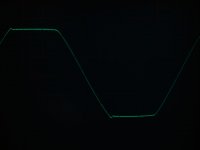
Attached a snapshot of 20kHz sine waves clipped.
This may be the first time that the result of simulation is close to what I observe in reality.
I found out that the capacitor labeled "Cx" in Michael's paper (e.g. in figure 57) is incredibly useful with TPC.
In the loopgain analysis, this seems to have roughly the same impact like the shunt compensation of the input LTP (C80 / R80), but it works differently and brings stability with TPC, whereas the shunt across the LTP does not.
Another very helpful addition is lead compensation across the feedback resistor.
I have this from Michael's paper as well.
I added 33pF and 1k.
I also found out that stability is far better with the TPC resistor being connected to Vcc instead of ground.
Connecting the resistor to ground obviously not only ruins PSRR, but also the compensation.
While the latter isn't obvious from simulation, at least to me, it showed on the bench.
Current values of the compensation are:
Cx (Michael) = 100pF
C85 (Miller) = 150pF
C84 (TPC) = 560pF
R84 (TPC) = 2k2
This gives roughly 400kHz UGLF and still 40dB OLG at 20kHz.
Not too bad for such a powerful amplifier.
I hope I can keep it that way.
I also further increased the shunt compensation inside the DBT from 1n5 to 3nF.
This dramatically reduced likelyhood of MHz ringing during clipping.
3nF is a lot of capacitance and going higher would (further) cut into phase margin.
I reduced the gate stoppers at the input of the diamond buffer from 100R to zero.
They don't seem to be required here, but may add phase shift.
Also, without the base stoppers, the shunt capacitor C82 is more available to the OPS and this capacitor helps to stabilize it.
The shunt compensation of the clipped signal (R83 / C83) does not seem to be required with TPC. Removed it for now.
Without any load, the amp seems somewhat stable now even when clipping, but adding an 8R load introduces some MHz ringing, 4R load makes it worse.
I can reproduce this in simulation by lowering the shunt inside the DBT from 3nF to 1n5.
Ringing only shows on the positive half wave of the signal in simulation and only on the negative half wave in reality.
Looking at the MJL3281 and MJL1302 datasheet, the MJL1302 has higher capacitance than the MJL3281.
At 2V, which is roughly the minimum Vce the clipping circuitry allows, this would be 6nF for the MJL3281 and 9nF for the MJL1302. And this is to be multiplied by four transistors for the complete OPS.
This could help to explain why ringing on the negative half wave is worse, but doesn't explain why it is vice versa in simulation.
Small signal square waves show a little overshoot (one small peak only, no undershoot, no ringing).
A slight overshoot is also present when entering clipping (at 20kHz sine waves).
This may have been there before, but I may not have noticed it because I was testing at 1kHz so far.
The amp does not break into 200kHz oscillation on power up and down anymore.
However, when overdriving the amp even more, the oscillation during clipping gets worse and lower in frequency. Might be 200kHz again, need to investigate further.
I suspect that shifting of transistor parameters somewhere in the OPS under load may cause the MHz instability I'm still having.
Just a theory, but it makes sense somehow.
Attached a snapshot of 20kHz sine waves clipped.
This may be the first time that the result of simulation is close to what I observe in reality.
Attachments

I believe at this point I should concentrate on the OPS.
BTW: This is interesting for everyone trying to get a triple emitter follower stable:
http://www.synaesthesia.ca/YAPOPstage.html
BTW: This is interesting for everyone trying to get a triple emitter follower stable:
http://www.synaesthesia.ca/YAPOPstage.html
Kiwanuka's Cx is there to get equal rolloff on both sides of the differential VAS. Symmetrical Miller caps won't work as expected because the mirror has a low impedance on the input side, so the voltage gain at that node is low. I didn't realize that when I designed my HPA2 amplifier, though what I ended up with seems to work ok. Kiwanuka explains this in his paper, so apologies if I'm stating the obvious.
He also talks about the DCDS circuit not having VAS buffers, but the Cordell front end does have them. They're used for the CMCL, but I expect they also perform the same function as in Self's EF-VAS. So some of Kiwanuka's analysis may need to be adjusted.
Simulation with my HPA confirmed that things worked better with low-value base stoppers at the output, and an RC shunt at the diamond buffer input, per your web page on the topic.
Thank you very much for your thoughts. Highly appreciated! Seems this cannot be stressed enough. Repeated in common language, I even get the point of capacitor Cx now.
In which way would Michael‘s analysis maybe need to be adjusted when having buffers like Bob‘s CMCL buffer?
At the moment, I’m investigating the DBT in more detail.
Seems like I’m not the first having issues with this:
https://www.diyaudio.com/community/threads/issue-with-3ef-diamond.278494/I did some simulation of the DBT earlier and the results looked promising, but when adding some inductance that is likely present in reality, the DBT becomes much harder to tame.
I suspect I might be having similar issues like Alan had seven years ago.
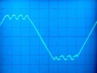
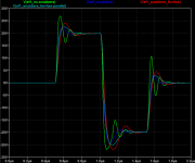
It seems like the issues I experienced with my diamond buffer output stages is exactly what Alan encountered as well earlier. The solution proposed is to put resistors of roughly 100 Ohm in series with the pre-drivers collectors of the DBT. This seemed to have worked well for Alan and Edmond made similar observations. My earlier experience with putting such a resistor into the simple class A biased diamond buffer confirms this. Roughly 10 Ohm seem just right in this application. However, in my DBT, those collector resistors don’t work as expected. I tried 100 Ohm. Connecting the pre-drivers collectors to the opposite supply instead cures the weird oscillation.
Please find attached two screenshots showing behavior during clipping with the pre-drivers connected to the next stage emitters (i.e. bootstrapped) and another with the collectors connected to the opposite power supply rails.
Please find attached two screenshots showing behavior during clipping with the pre-drivers connected to the next stage emitters (i.e. bootstrapped) and another with the collectors connected to the opposite power supply rails.
Attachments

Bootstrapping the pre-drivers would allow to use high performance low voltage transistors in theory that perform well in very low Vce application. However, they need good thermal coupling to the driver transistors so should have a package that allows easy thermal attachment. I find this difficult with TO-92 packages and therefore prefer a TO-127 package. There are some good high voltage transistors available in this package, but such transistors typically don’t do well at low Vce. So I chose BD139 / BD140 transistors, which are slow and have low hfe. Maybe losing the bootstraping and in turn using better (high voltage) transistors may even be an upgrade.
Conclusion at this point is that the issues I was dealing with stem from the driver and output stage arrangement and the front end wasn’t to blame apart from poor compensation maybe.
I simulated and experimented a bit to further stabilize the DBT output stage.
Conclusion is that the base to collector snubbers at the power transistors are good.
Better component values are 33R and 1nF instead of 100R and 47pF I had before. The previous values were never engineered, but blindly copied from Bob's HexFET OPS (where they likely make sense).
I reduced the drivers snubber caps to 1n5 without compromising stability. 3nF was really excessive.
As you can see in the previously posted scope screenshots, there is still some tiny oscillation present on the negative clipped edge.
I experimented a bit to figure out how to tame this.
The best result was achieved by adding ferrites in between the driver module and the OPS module.
I had some Würth 742701121 at hand.
With the ferrites added, the sustained oscillation is gone and just a bit of (lower frequency) ringing following entry of clipping remains.
Adding two ferrites in series does not further improve anything, but adds some minor ringing to the positive half wave.
I thought about trying ferrites for some time now, but simulation suggests that this is a bad idea.
In reality however, the result looks promising.
Square wave overshoot is unaffected with the measurement capabilities I have (which is a 1kHz square that produces only 6Vpp at the amp output).
I'm currently looking for a proper signal generator to improve my measurements.
Maybe I pick up the idea of putting small ferrites in series with each base stopper of the power transistor again...
What do you think about ferrites?
What is your experience?
Attachments

More ideas regarding ferrites:
I bought some Kemet B-20L-48B-L earlier for maybe putting them on the transistors terminals like that:

However, since I'm also having the snubbers from base to collector, the ferrites would counteract the snubbers when being put in between the snubber and the transistor.
This leads to the idea of putting the ferrite in series with the base stoppers like that:

The B-20L-48B-L has a characteristic that seems suitable to me.
Low impedance at 1MHz and reasonably high impedance at higher frequency:

I bought some Kemet B-20L-48B-L earlier for maybe putting them on the transistors terminals like that:
However, since I'm also having the snubbers from base to collector, the ferrites would counteract the snubbers when being put in between the snubber and the transistor.
This leads to the idea of putting the ferrite in series with the base stoppers like that:
The B-20L-48B-L has a characteristic that seems suitable to me.
Low impedance at 1MHz and reasonably high impedance at higher frequency:
Perhaps this is can be a reference at certain extend.... Harman Kardon HK990 also has ferrite beads over the base stopper resistor at the output transistors base, where the base stopper resistor itself, at a value of 10-ohms, works as a damping resistor to reduce the Q factor of the FB.

I noticed 3S5 ferrite material is selected for its lower-ish frequency range application, up to 30MHz. The 3S5 FB has a nominal impedance of 10-ohms at 1MHz.
Also can be noticed, in the datasheet attached, is that the impedance of a FB drops as the DC bias current it passes increases, what they call DC premagnetization, significantly when the DC current exceeds a certain level, say 0.5A, indicating saturation.
Attachments
Hi Nattawa,
thanks for your input.
This is really helpful!
I didn't have the idea to parallel the base stopper with ferrites yet, but this looks most promising.
Damping is something I was concerned about. Ferrites have an inductive part as well and this may be significant.
With the parallel resistor (just like the output filter of the amp) the Q is well controlled.
Another advantage of the parallel arrangement would be better current sharing of the power transistors since the base stoppers counteract the balancing effect of the emitter resistors.
I thought that the base stopper in series with the ferrites also lowers Q, but this seems less effective than with the parallel arrangement.
Unfortunately it seems a little known fact that ferrites saturate because most datasheets omit this information, just like the inductive contribution to Z is often not shown.
I've seen such a tiny ferrite on a drain terminal of a commercial product somewhere here in the forum.
Once there is significant Ic flowing, the tiny ferrite becomes pretty much useless.
May be desired in that application, who knows?
I did a simulation in order to align my observations in reality with the theory.
Adding ferrites contributed to stability in reality, but simulation says otherwise.
In reality, not only the faint ringing was gone, but also I was able to load the NFB node with more capacitance.
When playing small square waves and I put 4n7 at the NFB node, the amp bursts into oscillation.
This behavior seems pretty binary because at 1n5, the amp doesn't care.
I would have expect some more overshoot at the corners followed by some ringing.
However, with the ferrites in place, the amp doesn't care about 4n7 and it takes 6n8 to provoke oscillation.
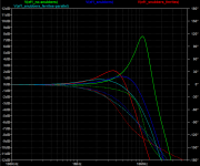
Here are some plots from simulation of the power output stage only (EF1) driven by a voltage source with 1R output impedance, illustrating four cases:
1. No snubbers (green)
2. 33R and 1n base to collector snubbers (blue)
3. same snubbers and 74276031 ferrites in series with each 2R2 base stopper (red)
4. same snubbers and 74276031 ferrites in parallel with each 10R base stopper (petrol)
Ferrite datasheet for convenience: 74276031 Würth Elektronik
thanks for your input.
This is really helpful!
I didn't have the idea to parallel the base stopper with ferrites yet, but this looks most promising.
Damping is something I was concerned about. Ferrites have an inductive part as well and this may be significant.
With the parallel resistor (just like the output filter of the amp) the Q is well controlled.
Another advantage of the parallel arrangement would be better current sharing of the power transistors since the base stoppers counteract the balancing effect of the emitter resistors.
I thought that the base stopper in series with the ferrites also lowers Q, but this seems less effective than with the parallel arrangement.
Unfortunately it seems a little known fact that ferrites saturate because most datasheets omit this information, just like the inductive contribution to Z is often not shown.
I've seen such a tiny ferrite on a drain terminal of a commercial product somewhere here in the forum.
Once there is significant Ic flowing, the tiny ferrite becomes pretty much useless.
May be desired in that application, who knows?
I did a simulation in order to align my observations in reality with the theory.
Adding ferrites contributed to stability in reality, but simulation says otherwise.
In reality, not only the faint ringing was gone, but also I was able to load the NFB node with more capacitance.
When playing small square waves and I put 4n7 at the NFB node, the amp bursts into oscillation.
This behavior seems pretty binary because at 1n5, the amp doesn't care.
I would have expect some more overshoot at the corners followed by some ringing.
However, with the ferrites in place, the amp doesn't care about 4n7 and it takes 6n8 to provoke oscillation.
Here are some plots from simulation of the power output stage only (EF1) driven by a voltage source with 1R output impedance, illustrating four cases:
1. No snubbers (green)
2. 33R and 1n base to collector snubbers (blue)
3. same snubbers and 74276031 ferrites in series with each 2R2 base stopper (red)
4. same snubbers and 74276031 ferrites in parallel with each 10R base stopper (petrol)
Ferrite datasheet for convenience: 74276031 Würth Elektronik
Attachments
Last edited:
I experimented with adding ferrites to the output stage and here are my results:
Adding bespoke Kemet ferrites in series with each base stopper resistor did not show significant effect in reality.
I received some free samples of WAFB ferrites from Würth Elektronik and installed 7427605 ferrites with 12R resistors in parallel.
I chose the stronger ferrites because the weaker ones (in series) did not show enough effect.
Actually I have many of those in parallel compared to the single 742701121 I used on the common drives for the whole OPS.
The parallel arrangement cured the faint oscillation.
I bought a better DAC, which allows higher frequency and higher level output and now clipping at 40kHz, there is some tiny ringing (only a few cycles) following entry of clipping, but this is barely visible in the milliVolt range.
Conclusion is that all the snubbers are essential for a stable triple and the ferrites added further refinement.
Another conclusion is that the compensation of the front end cannot fix an unstable output stage being included in the negative feedback loop.
Since the triple OPS is somewhat stable now, I feel adventurous introducing new potentially unstable features to the front end.
Michael's paper inspired me with what he calls "input differential cascodes".
Which is basically driving the cascode of each LTP transistor from each emitter individually.
There is an interesting discussion about driven cascodes here: Bob Cordell's amplifier book - driven cascodes for the LTP
In another discussion, which I'm unable to find again, the conclusion was that the effect of the driven cascode is negligible in simulation, likely due to poor modeling of Vce dependent non-linearity of some transistor models.
But in reality, this might reduce distortion without pushing compensation into the danger zone.
Stealing current somewhere from the tail or emitter and adding capacitance at this place is not without risk however.
I'm running my tail at 8mA, which may help a bit.
And I found base stoppers for the level shifter transistors help to isolate the input capacitance of those transistors.
Does anybody have practical experience with what I'm planning to do?
Or food for thought?
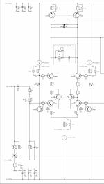
Attached a snip of the schematic illustrating how I plan to approach the driven cascodes.
Since the triple OPS is somewhat stable now, I feel adventurous introducing new potentially unstable features to the front end.
Michael's paper inspired me with what he calls "input differential cascodes".
Which is basically driving the cascode of each LTP transistor from each emitter individually.
There is an interesting discussion about driven cascodes here: Bob Cordell's amplifier book - driven cascodes for the LTP
In another discussion, which I'm unable to find again, the conclusion was that the effect of the driven cascode is negligible in simulation, likely due to poor modeling of Vce dependent non-linearity of some transistor models.
But in reality, this might reduce distortion without pushing compensation into the danger zone.
Stealing current somewhere from the tail or emitter and adding capacitance at this place is not without risk however.
I'm running my tail at 8mA, which may help a bit.
And I found base stoppers for the level shifter transistors help to isolate the input capacitance of those transistors.
Does anybody have practical experience with what I'm planning to do?
Or food for thought?
Attached a snip of the schematic illustrating how I plan to approach the driven cascodes.
Attachments
- Home
- Amplifiers
- Solid State
- VFA front end - the Bunnyphant