Mostly anyway in case of different enclosures we need to put a differential receiver in the front of amplifier.External case, but no long cables between (>1m).
.png")
.png")
No, it needed only as "grid leak" for keeping output low in case of disconnecting from preamplifier of powered amp and doesn't work at all being connected (it will be shunted by low output impedance of preamp's output).Thought 10k would be a appropriate input impedance, like to keep as low as possible.

I'm still reading 🙂
Why not build an original as it was well received and proven and then work on something that might better it 🙂 You then have the original to compare against.
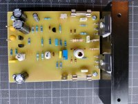
Well, I just did. Finally got some time to work on this project so build the original circuit, only modified slightly for +/- 25 V. Never thought that it would perform near the spice simulations, but the results were quite disappointing i think.
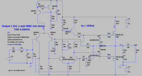
- THD 0,053 % 1kHz, 1 W 8 ohm
- THD 0,081 % 1kHz, 16 W 8 ohm
- THD 0,75 % 1kHz, 25 W 8 ohm
- Slew rate about 20V/µS (OK I think)
- Input sensitivity 1,3 Vpp for 25W output into 8 ohm (had to change R6 to 1k from 1k2)
All measurements were done with a bias current of 105 mA, haven't tried to change it yet cause I want to compare it with the next version I build. Unfortunately I don't have a low distortion 20kHz signal source, so I can't measure the distortion at other frequencies. But I can only assume that it will be worse.
Interesting that I found the (almost) same circuit in R Slone's book "High-Power Audio Amplifier Construction Manual". In the book he states that the performance of the amp is below 0,1 % at 1 khz, but quickly begins to deteriorate reaching 2% THD at 20 kHz. Sounds same as for my prototype... I wonder why the spice simualtion differ that much from real circuit in this matter, but that's for another thread to discuss I guess.
Attachments
After I lot of playing around with LT spice, trying to make use of all the tips I've got so far, I think that the two pole compensating VAS is by far the best improvement. Thanks, @HAYK ! It greatly reduces the distortion at high frequencies, which I believe from previous spice simulations (and reading R Slone's book) is the biggest down side with this amp.
However, the altering the values of the caps and resistor int eh two pole network doesn't seem to have any big effect the distortion, ending up around 0,004 % at 20 W 20kHz. Bigger caps kills affect the slew rate of course. 22p/220p + 2k2 simulates slewrate at 45V/µS and increasing it to 68/680p + 4k7 drops it to 30V/µS. 22p sounds really low to me, but since it simulates ok I think I will try to build it as this;

Choosed to keep the CCS for the input stage, since it did improve the perfomance in simulation for me. Will be interesting to see if it performs better than the previous "original" amp. Also added the zenerdiodes for protection, limiting the current to 8 amp or so in a worse case situation.
However, the altering the values of the caps and resistor int eh two pole network doesn't seem to have any big effect the distortion, ending up around 0,004 % at 20 W 20kHz. Bigger caps kills affect the slew rate of course. 22p/220p + 2k2 simulates slewrate at 45V/µS and increasing it to 68/680p + 4k7 drops it to 30V/µS. 22p sounds really low to me, but since it simulates ok I think I will try to build it as this;
Choosed to keep the CCS for the input stage, since it did improve the perfomance in simulation for me. Will be interesting to see if it performs better than the previous "original" amp. Also added the zenerdiodes for protection, limiting the current to 8 amp or so in a worse case situation.
Attachments
Hard to say... PCB layout will be very important ultimately as will ground returns (not to cast aspersions on your set up 🙂)
One thing that immediately jumps out is that the gate stopper resistors should be mounted on the FET gate itself and not at the board end of the wire. That is very important generally with any FET amp. In fact I don't see them in your circuit diagram.
This is from the Maplin articles so this would be actual measurement :
Well, those number match up better with the spice simulations. And compared to other MOSFET amps I've seen very impressive. Way better than Slone's too, may I ask where from this articles is?
About the gate stoppers, I be leave this is R13 and R14 in the attached PDF schematic in post #62. Slone doesn't include them in his version, strange. The plan was to mount the transistors at the board in, and if so the resitors would be pretty close to the gates. But then I threw it on that big heatsink just for testing, unknowing of this isseu. Maybe I should try to solder them at the gates just for testing...
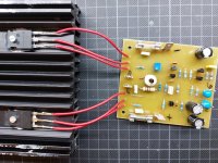
PCB design is of course very important. And I'm not an expert on this topic, still learning. So attached is the PCB that I designed (quite quickly), feel free to comment it if you like. Note that the signal ground (GDNS) and power ground are separated at the board. The plan is to connect them separately to a central ground star outsides the board later (though, then I tested the board I just connected then with a alligator clip).
About the gate stoppers, I be leave this is R13 and R14 in the attached PDF schematic in post #62. Slone doesn't include them in his version, strange. The plan was to mount the transistors at the board in, and if so the resitors would be pretty close to the gates. But then I threw it on that big heatsink just for testing, unknowing of this isseu. Maybe I should try to solder them at the gates just for testing...
PCB design is of course very important. And I'm not an expert on this topic, still learning. So attached is the PCB that I designed (quite quickly), feel free to comment it if you like. Note that the signal ground (GDNS) and power ground are separated at the board. The plan is to connect them separately to a central ground star outsides the board later (though, then I tested the board I just connected then with a alligator clip).
H
HAYK
Instead of CCS, which defigures the original circuit, you can use the bootstrap. Split the 68k into 10k+56k and bring from output 1uF+ 9xR8 that is 220k to the joint so that it is nearly equal to the feedback ratio 27k/1k. By this, when the input voltage is 2v for ex, the feedback is 2v and the emitters follow too so that the current through 56k remains constant.
Already etched a board for the the CCS version in post #63, so I'll probably build it anyway. But I always found it interesting to learn new things, maybe I can modify the board I just built for boot-strapping.
However, I'm not sure exactly what you suggest (not sure which schematic you refereed to either). This is that I tried, changed the values some to make it work with my 25V version. Simulates pretty good, THD is now only 0,003%. May have to try this... did I get it right?

However, I'm not sure exactly what you suggest (not sure which schematic you refereed to either). This is that I tried, changed the values some to make it work with my 25V version. Simulates pretty good, THD is now only 0,003%. May have to try this... did I get it right?
H
HAYK
I tried upon the precedent circuit with resistor 12k, with bootstrap as shown and with CCS 2ma. The result for 1w 1khz is 0.0005%, 0.000466, 0.000463. Does it worth to replace a single resistor for just 0.000034% less.

Attachments


Regarding post #68 if I'm right R8-D1/R11-TR5 forms a current mirror.
If yes, why "deform" it and not use 2 pieces of 2N5401 with the same resistor values?
(Like in the popular "symasym" design.)
If yes, why "deform" it and not use 2 pieces of 2N5401 with the same resistor values?
(Like in the popular "symasym" design.)
... and received the necessary phase frequency characteristic for stable operation. Added the mirror.After I lot of playing around with LT spice...
Attachments
Well, I done it again. Built a beautiful oscillator today instead of an amp. Finished the board based on schematic in post #68. Adjusted the bias current and everything seems ok, offset was about 2 mA but the output was oscillating... don't know why, tried to increase the compensating caps to 68/470p, but no improvement.

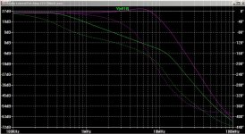
This is a little outside my knowledge at them moment. Wish I knew more about how to predict the stability of an amp based on spice simulations. I'll study your simulation more closely.
No, your figures are really impressive. Reason I choose the CCS was because (I thought) I knew that I was doing. But I didn't... Doubt that I get it working actually so maybe a good idea to move back towards the original circuit, that I actually got working OK.
I see now that I connected R18 (referring to your schematic post #69) to the wrong point now. And what C9, 100µF? Thought 1µF first. Since it will be a polar cap in reality, which way should it be connected? Guessing that postive end should be connected to R3/R17 and negative to R9?
... and received the necessary phase frequency characteristic for stable operation.
This is a little outside my knowledge at them moment. Wish I knew more about how to predict the stability of an amp based on spice simulations. I'll study your simulation more closely.
I tried upon the precedent circuit with resistor 12k, with bootstrap as shown and with CCS 2ma. The result for 1w 1khz is 0.0005%, 0.000466, 0.000463. Does it worth to replace a single resistor for just 0.000034% less.
No, your figures are really impressive. Reason I choose the CCS was because (I thought) I knew that I was doing. But I didn't... Doubt that I get it working actually so maybe a good idea to move back towards the original circuit, that I actually got working OK.
I see now that I connected R18 (referring to your schematic post #69) to the wrong point now. And what C9, 100µF? Thought 1µF first. Since it will be a polar cap in reality, which way should it be connected? Guessing that postive end should be connected to R3/R17 and negative to R9?
Attachments
H
HAYK
You can transform the IPS current mirror into double CCS.... and received the necessary phase frequency characteristic for stable operation. Added the mirror.
Post in thread 'VAS requirements for MOSFET OPS' https://www.diyaudio.com/community/threads/vas-requirements-for-mosfet-ops.404529/post-7486666
Well, I done it again. Built a beautiful oscillator today instead of an amp.
i keep seeing people going from sims straight to pcb, usually with issues.
why not build a point-to-point prototype first, since as with this circuit, it is not overly complex.
in spice sims you can connect transistors upsidedown and insideout and the circuit still "works"
According to the photo of the board, there is only one compensation capacitor. If VAS is a differential pair, both transistors require compensation capacitors of the same value.tried to increase the compensating caps to 68/470p, but no improvement.
Also, as Cortez mentioned, R8 and R11 should be the same value. D1 can be left alone.
I totally agree. We recommend assembling with perfboard first.why not build a point-to-point prototype first, since as with this circuit,
at this point, it would be useful to read the original papers about this from the old Hitachi data book or even the original circuit with the original prototype lateral mosfets (published in the IEEE journal of consumer electronics, i think in 1978). among other things, that info shares some parameters to be considered for the driver transistors choice and the use of a damped inductor at the output being critical for low distortion at higher frequencies. study the circuits Hitachi used in actual released products based on this topology for tips/hints.
The oscillations was the mostly due to the two pole compensated VAS. Tried it without it and it worked again. For some reason the CCS version appears to be more picky about the capacitor values. Found out that 47p was about the right. Greater values of course slow down the slew rate. Also tried a bootstrap version, with the rest of the values as original.
But there's nothing that really beats the original circuit. had to measure it again, cause I had a hard time believing those numbers and they were better next time for some reason. Here's some comparisons if anyone interested;
"Original" circuit;

THD 0,02% at 1W 1kHz 8 ohm
THD 0,06% at 26W 1kHz 8 ohm
Slew rate 20V/µS
With CCS;

THD 0,01% at 1W 1kHz 8 ohm
THD 0,08% at 30W 1kHz 8 ohm (don't why I could push it to 30 W now...)
Slew rate 16V/µS
Bootstrapped;

THD 0,015% at 1W 1kHz 8 ohm
THD 0,06% at 25W 1kHz 8 ohm
Slew rate 20V/µS
Interesting how the Spice simulations actually differs from reality. Also I noted that offset was about -2-3mV for all amps, regardless of that the simulations sad.
According to these measurement I would say that the original circuit performs best so far, maybe a descent amp actually. What bothers me is that the distortion will probably increase a lot at higher frequencies. So a way to reduce this is needed... don't know why I didn't work with two pole compensation. Have to work on this.
But there's nothing that really beats the original circuit. had to measure it again, cause I had a hard time believing those numbers and they were better next time for some reason. Here's some comparisons if anyone interested;
"Original" circuit;
THD 0,02% at 1W 1kHz 8 ohm
THD 0,06% at 26W 1kHz 8 ohm
Slew rate 20V/µS
With CCS;
THD 0,01% at 1W 1kHz 8 ohm
THD 0,08% at 30W 1kHz 8 ohm (don't why I could push it to 30 W now...)
Slew rate 16V/µS
Bootstrapped;
THD 0,015% at 1W 1kHz 8 ohm
THD 0,06% at 25W 1kHz 8 ohm
Slew rate 20V/µS
Interesting how the Spice simulations actually differs from reality. Also I noted that offset was about -2-3mV for all amps, regardless of that the simulations sad.
According to these measurement I would say that the original circuit performs best so far, maybe a descent amp actually. What bothers me is that the distortion will probably increase a lot at higher frequencies. So a way to reduce this is needed... don't know why I didn't work with two pole compensation. Have to work on this.
Attachments
According to the photo of the board, there is only one compensation capacitor. If VAS is a differential pair, both transistors require compensation capacitors of the same value.
Also, as Cortez mentioned, R8 and R11 should be the same value. D1 can be left alone.
The VAS is a differential pair I be leave. So if these transistors require the same compensating capacitor, does that also apply for two pole compensating networks?
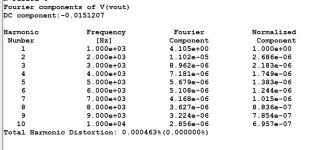
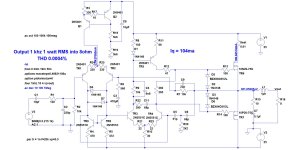
Redesigned the original VAS circuit to (another) two pole compensating network. And think I got it working now, needs a little tweaking but numbers are quite impressive so far; 0,00015 % THD at 1kHz at 1 W, and only 0,003% at 20kHz.

Attachments
So if these transistors require the same compensating capacitor, does that also apply for two pole compensating networks?
Yes, you need to compensate both sides of the differential pair to do it correctly. Therefore, for a differential pair, four capacitors and two resistors are required.
Yes, I think the circuit configuration #79 is fine. However, I think the values need to be adjusted. I think the unity loop gain is too high.
Last edited:
- Home
- Amplifiers
- Solid State
- VAS requirements for MOSFET OPS