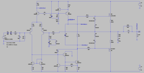
What are the requirement for the VAS driving a MOSFET source-follower OPS? Currently I'm trying to design my first MOSFET poweramp, aiming for about 20W RMS using lateral MOSFET:s (very low power for these output devices, but I have a 2x18 V transfomrer I intend to power it with). Basically what I've done is that I used the design from an other amp I'v built and "just" replaced the the OPS with MOSFET. Spice simulation gave ok results.

But then I thought, since MOSFET OPS doesn't need that much current, maybe I can use a simplier VAS? The benefits of this Darlington-arrangment basically only applies then using BJT OPS, which requivere quite high currents (?). So I tried it in Spice too. This time with only one transistor. I had to increase the current for the input stage, since it takes more current to drive it. But what I found interesting is that it did performed about as good as the Darlington arrangement in terms of distortion and slew rate, according to Spice.

The results from Spice simulation is quite impressive, around 0,001 % THD @ 1kHz 1W into 8 ohms, increasing to about 0,03 % at 20 W. Though, I doubt that the actual amp will perform as this good if I built it.
So could I use the single transistor VAS instead, or is there anything else I'm missing here?
But then I thought, since MOSFET OPS doesn't need that much current, maybe I can use a simplier VAS? The benefits of this Darlington-arrangment basically only applies then using BJT OPS, which requivere quite high currents (?). So I tried it in Spice too. This time with only one transistor. I had to increase the current for the input stage, since it takes more current to drive it. But what I found interesting is that it did performed about as good as the Darlington arrangement in terms of distortion and slew rate, according to Spice.
The results from Spice simulation is quite impressive, around 0,001 % THD @ 1kHz 1W into 8 ohms, increasing to about 0,03 % at 20 W. Though, I doubt that the actual amp will perform as this good if I built it.
So could I use the single transistor VAS instead, or is there anything else I'm missing here?
Attachments
D
Deleted member 550749
They will be running a couple of 100ma bias current at that gate voltage.
I would recommend you try without the 0.22 ohms (not needed for laterals with their negative tempco) and also remove the vbe multiplier (not needed as temp compensation) and just use a resistor to set the bias current.
I would recommend you try without the 0.22 ohms (not needed for laterals with their negative tempco) and also remove the vbe multiplier (not needed as temp compensation) and just use a resistor to set the bias current.

The current requirement depends on the max dV/dt you want to handle and the combined capacitance of the output MOSFETs. 6mA is probably enough for a pair of laterals with their 600--800pF or so. Too little drive current and it will slew-limit.What are the requirement for the VAS driving a MOSFET source-follower OPS?
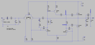
But then I thought, since MOSFET OPS doesn't need that much current, maybe I can use a simplier VAS? The benefits of this Darlington-arrangment basically only applies then using BJT OPS, which requivere quite high currents (?).
By Darlington VAS do you mean one with an emitter follower? The first device's collector is usually tied to ground, not to the second devices collector, so its not a Darlington pair. The point is to avoid the non-linear Miller capacitance of the first device. Nothing to do with driving BJT OS.
They will be running a couple of 100ma bias current at that gate voltage.
100mA sound a little hot, but ok (at least for a newbie like me). Haven't really played with the bias yet. Chose a bias voltage of about 1,1 V to start with (from Randy Slone's book high power amplifier construction manual).
would recommend you try without the 0.22 ohms (not needed for laterals with their negative tempco) and also remove the vbe multiplier (not needed as temp compensation) and just use a resistor to set the bias current.
Yes, don't know why I didn't think of it. The vbe multiplier is of course not needed. Also the capacitor across is way to big I be leave (?), since were is not that much variation in currents now through the bias resistor as with BJT as OPS. Tried to lower it to 470nF and couldn't se any differences.
Didn't know about the 0.22 ohms resistor. A lot of designs (Slone's for example) seems to have them anyway. The only disadvantageous is the power loss I guess. Also very handy to measure across with the multi-meter then setting the bias current.
The current requirement depends on the max dV/dt you want to handle and the combined capacitance of the output MOSFETs. 6mA is probably enough for a pair of laterals with their 600--800pF or so. Too little drive current and it will slew-limit.
Aha, this makes sense. So I tried to increase the current of the VAS in order to improve the slew rate. With the single transistor VAS this did not work as weel, since the extra current neede from the input stage affected the whole DC balance of the amp and also had a negative impact of the distoriton.
However with the first VAS I was able to increase the current to 9,5 mA without ruin the DC balance to much. And slew rate improved a bit from 10V /µS to about 13VµS. Also distortion got lower, from about 0,009 to 0,006 % THD at 1 kHz 1 W 8 ohm.
By Darlington VAS do you mean one with an emitter follower? The first device's collector is usually tied to ground, not to the second devices collector, so its not a Darlington pair. The point is to avoid the non-linear Miller capacitance of the first device. Nothing to do with driving BJT OS.
Well, yeah I got a little mixed up last night. The arrangement of the first schematic is usally refered to as "Darlington VAS" in some books. But your're right it has nothing to with BJT OPS. The benfeits are that beta enhancment of using to transistors. I only (almost) only seen practical examples of on transitor VAS used in MOSFET amps.
Attachments
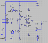
Hitachi did a lateral mosfet circuit way back in 1970's.
Simulated in Spice. Changed the feedback resistor to lower the gain and get the DC balance ok, -1.7 mV is acceptable I guess. Like the simplicity of the circuit and according to spice it performs ok actually. THD is 0,008% at 1kHz at 1W into 8 ohm. Increases to about 0,02 % THD at 10kHz at 20W.
And slew rate ok, about 12V/µs. Some ringing though.
By the results of spice simulation, maybe I should build this one instead....
Attachments
And slew rate ok, about 12V/µs. Some ringing though.
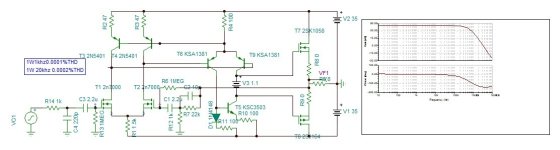
The square wave generated in LT has 'infinite' rise time. Try making C2 a 470pF.
Really fun circuit.Simulated in Spice. Changed the feedback resistor to lower the gain and get the DC balance ok, -1.7 mV is acceptable I guess. Like the simplicity of the circuit and according to spice it performs ok actually. THD is 0,008% at 1kHz at 1W into 8 ohm. Increases to about 0,02 % THD at 10kHz at 20W.
And slew rate ok, about 12V/µs. Some ringing though.
View attachment 1225310
By the results of spice simulation, maybe I should build this one instead....
One of my favorites.
For actual project usually replace R3 47k with constant current source of 1.7 to 2ma.
And R4/5 can be fine tuned to 2.7k to 3.3k to get Q3/Q4 current ideal.
If the gain is lowered and lower value resistors used for R6/R7 1k/22 to 27K with
larger cap. should sim well and lower distortion.
have also used KSA/KSC 3503/1381 for Q3/4/5 and adjust R4/5 to get current
to 6 to 7 ma no higher /lower for best performance.
to fine tune DC offset like the original they have different value for R2 instead
of matching R7 as usually done.
Or slightly lower/ raise R9 10k to 12k usually about the best.
Very fun circuit, performs well with low parts count.
Instead of 2n5401 for pnp input can also try usual BC556 or KSA992
again feed by constant current source usually 1.5 to 2ma.
and 2.7 , 3.3 to 3.9K to get next stage current correct/ fine tuned
Mosfet bias typically hot around 100ma for better slew/high frequency
lower crossover distortion.
Otherwise for VAS in other topology to direct drive mosfet.
use TO-92 for beta enhancement and then drive KSC3503
with only 6 to 8ma needed.
Last edited:
Try this mirror-biased two-stage follower OPS.
It will greatly expand bandwidth, soften shoulder transition, allow for huge VAS loading resistor nominals and overall improvement in amplifier's open loop depth with corresponding lowering of THD figures.
It will greatly expand bandwidth, soften shoulder transition, allow for huge VAS loading resistor nominals and overall improvement in amplifier's open loop depth with corresponding lowering of THD figures.
Attachments
The square wave generated in LT has 'infinite' rise time. Try making C2 a 470pF.
Interesting, that took care of the ringing of the rising edge of the waveform. had to increase it to about 1nF to completely get rid of ti. Didn't thought about it, but usually set the rise rime to 1ns, thinking that it will not affect the results then.
For actual project usually replace R3 47k with constant current source of 1.7 to 2ma.
And R4/5 can be fine tuned to 2.7k to 3.3k to get Q3/Q4 current ideal.
Was thinking of it actually. Have to convert the circuit to run of +/-25 V anyway, so some resistors like R3 will have to adjusted.
Instead of 2n5401 for pnp input can also try usual BC556 or KSA992
again feed by constant current source usually 1.5 to 2ma.
and 2.7 , 3.3 to 3.9K to get next stage current correct/ fine tuned
Mosfet bias typically hot around 100ma for better slew/high frequency
lower crossover distortion.
Why not the 2n5401? Just curious. I have some matched 2n5401 that I want to use, so that's why I designed with them int he first place.
2N5401/5551 one my favorites as well.
Sounds great if you have matched pairs. definitely have fun with them.
I too like 25 to 35 volt rails.
Just mentioned other options.
In this voltage range all the classic known differential circuits using lower voltage/ low noise
transistors are feasible.
Just mentioned it, once you have a board.
Should be fun to play with. With a current source.
Basically any classic transistor will work. Since ideal current
about the same for all of them.
Not much of a surface mount guy, but 5401/5551 come
in matched pairs on same die as well.
Great for differential/mirrors.
Rather surface or through hole. Just a great part
to have.
This circuit is so fun to me, with good board.
Topology stays same, but values can be changed
to adapt to many transistors.
Would even like to find current produced
higher current T092-MOD package.
I like the extended larger cases for higher current
in a Vas section or current source.
Just fun options to play around with.
- Home
- Amplifiers
- Solid State
- VAS requirements for MOSFET OPS