Yeah, I seem to recall the regulator slipping into discontinuous mode at about 300 mA for my chosen inductance. DCM is a different animal when it comes to feedback and compensation.
Whether you need multiple regulators or just one depends on the amp design. Basically, if you can run the filaments using the same transformer winding, you can run them using the same regulator. Each regulator will need its own transformer winding.
For DHT's with one end of the filament grounded, you could try to run multiple tubes from the same regulator. I would expect better results (sound quality) by using multiple regulators, though. If the DHT's are using cathode resistors for the bias, each tube will need its own regulator.
~Tom
Sweet!
Perhaps you can provide an opinion here... The regulator itself takes up very little circuit board area. The input rectifier and reservoir cap take up about as much room as the regulator. Would you prefer a board with a rectifier or without?
Onboard rectifier would require only AC to run. The board without rectifier would require rectification to be done elsewhere and the board to be fed DC. The board with onboard rectifier would be roughly twice the board cost of a regulator-only board.
Others are welcome to chime in as well, of course.
I'm leaning in the direction of a regulator-only board. There are many different packages for rectifiers and reservoir caps, so arriving at a "one size fits all" is a challenge. And both rectifier bridges and reservoir caps have traditionally been chassis-mounted anyway.
The other advantage of regulator-only boards is that they stack nicely. I could probably stack 3~4 of them before running out of room in a 3" tall chassis.
~Tom
Personally, my requirement is for 7.5V @ 5A (four 841s) so I would prefer they be small and stackable so that I can divide the load between a couple of regulators. It really is easy to point-to-point wire the rectifiers on a terminal strip. Doing that on the board kind of restricts you to using parts that fit the board. My vote is for a regulator-only tiny board.
Tom,
With that much line regulation, there may be a 'system level' advantage in easing off the brute force characteristic of the mains rectifier stage (ie. soften the mains rectifier current pulses at the expense of mains ripple magnitude coming in to the post regulator, but possibly improvement in high frequency glitch feedthrough).
Tim
At 300ma it might be best to drop the inductance slightly to be sure to stay away from discontinuity as ripple may go up rapidly. Not a big issue with web bench available for modeling.
I can go with regulator only as well.
I can go with regulator only as well.
What is the minimum recommended load at 4V ?
Sorry. You said minimum. I read maximum and answered accordingly. I don't have an exact number for the minimum current but the 300 mA that's floating around sounds reasonable. I'd need to do the math on my component values, though.
~Tom
At 300ma it might be best to drop the inductance slightly to be sure to stay away from discontinuity as ripple may go up rapidly. Not a big issue with web bench available for modeling.
Exactly. Once I get further with the design, I plan to post a spreadsheet of recommended values.
The regulator deals with DCM fairly gracefully, but staying in CCM is preferable for many reasons. I have no issues with the regulators running without any load (other than the resistive feedback network). I'm not going to guarantee good performance at that operating point, though... 🙂
What's the nominal filament current on those 4P1L's?
Looks like there's consensus on doing a regulator-only board. I'm envisioning 2x2 inches (50x50 mm) or so. Maybe smaller. I'll see once I get mounting holes and connectors placed...
~Tom
Here is what I plan to support:
1.5 V @ 1.05 A (#26 tube)
2.5 V @ 2.5 A (2A3 tube)
4.2 V @ 325 mA (4P1L tube)
5.0 V @ 1.4 A (300B tube)
6.3 V @ 300 mA and up (various indirectly headed tubes)
7.5 V @ 1.25 A (801A tube)
12.6 V @ 150 mA and up (various indirectly headed tubes)
Let me know if you have other requests.
The regulator output voltage will be programmable by changing out a resistor.
The regulator can supply up to 3 A continuously. However, note that it does require a minimum current to be drawn for best performance. I would prefer a design that can handle a current range of, say 100 mA to 3 A, but if need be I may offer two tested designs - one that's optimized for a higher output current (say 1 A and up) and one that's optimized for low output current for operation in the range of 100 mA ~ 1 A. The switch from one current range to the other will require the inductor to be switched out.
~Tom
Latest developments
So... I played around with WebBench trying to find a good optimum. I discovered a few things.
1) I was running the LM22673 slightly above the recommended maximum of 180 uF for the output cap.
2) As a result, the control loop had pretty low phase margin, hence, poor transient response.
So, I swapped Cout for a 47 uF Murata X5R ceramic cap. The output ripple actually got lower (!) probably because the ceramic cap has a higher SRF (i.e. it works as a capacitor at the switching frequency). The transient response and output impedance improved as well.
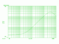
One trick I was taught regarding stability analysis was to look at the impedance of a node. If the node impedance has high-Q peaks in it, the circuit is likely unstable. With Cout = 200 uF, the Q was about 2. Now, with Cout = 47 uF, it's dropped to 0.67. This is supported by WebBench, which reports an improvement in phase margin from 40 degrees (Cout = 200 uF) to 58 degrees (Cout = 47 uF).
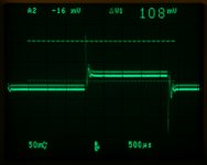
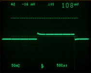
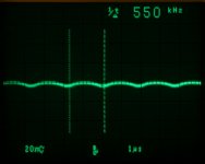
Attached shows the transient response with 200 uF and 47 uF. I'm not sure what causes the double-trace at 200 uF. Sorry about the voltage marker. That 108 mV means nothing. The ripple at 47 uF is shown as well (the ripple for 200 uF can be found in Post #69). Finally, the output impedance for 47 uF is shown.
The transient response was done with 1.25 A static current and a 63 mA step at 240 Hz or so. The output impedance was measured at 1.25 A static current and 94 mA RMS test signal.
~Tom
So... I played around with WebBench trying to find a good optimum. I discovered a few things.
1) I was running the LM22673 slightly above the recommended maximum of 180 uF for the output cap.
2) As a result, the control loop had pretty low phase margin, hence, poor transient response.
So, I swapped Cout for a 47 uF Murata X5R ceramic cap. The output ripple actually got lower (!) probably because the ceramic cap has a higher SRF (i.e. it works as a capacitor at the switching frequency). The transient response and output impedance improved as well.
One trick I was taught regarding stability analysis was to look at the impedance of a node. If the node impedance has high-Q peaks in it, the circuit is likely unstable. With Cout = 200 uF, the Q was about 2. Now, with Cout = 47 uF, it's dropped to 0.67. This is supported by WebBench, which reports an improvement in phase margin from 40 degrees (Cout = 200 uF) to 58 degrees (Cout = 47 uF).
Attached shows the transient response with 200 uF and 47 uF. I'm not sure what causes the double-trace at 200 uF. Sorry about the voltage marker. That 108 mV means nothing. The ripple at 47 uF is shown as well (the ripple for 200 uF can be found in Post #69). Finally, the output impedance for 47 uF is shown.
The transient response was done with 1.25 A static current and a 63 mA step at 240 Hz or so. The output impedance was measured at 1.25 A static current and 94 mA RMS test signal.
~Tom
Attachments
Last edited:
If you just swapped output C, then that clearly indicates the ESL of the electrolytic. Ceramic smt would have to be the best option at any time you can physically stack it - maybe difficult for production, but manually stacking large smt format ceramics is always a neat method.
You should get some switching transient improvement from smaller footprint smt ceramic caps on input and output, probably placed on the underside, with the smallest loop distance of the switching loops.
Ciao, Tim
You should get some switching transient improvement from smaller footprint smt ceramic caps on input and output, probably placed on the underside, with the smallest loop distance of the switching loops.
Ciao, Tim
If you just swapped output C, then that clearly indicates the ESL of the electrolytic. Ceramic smt would have to be the best option at any time you can physically stack it - maybe difficult for production, but manually stacking large smt format ceramics is always a neat method.
If you look at the first step response o'scope picture, you'll notice an extreme spike followed by 10-ish kHz ringing. The extreme spike, I bet is the ESL of the 'lytic. But the ringing is loop behavior.
I wasn't clear in my post above, but the 200 uF I used was actually 47 uF X7R ceramic + 150 uF electrolytic (one of the modern 7 mOhm ESR types by Nichicon). For the experiments with just 47 uF I removed the 150 uF cap and left the 47 uF ceramic cap in place.
I don't need to stack the caps. The output lead from the inductor is almost 10 mm wide, so I can put several ceramic caps side-by-side. But of course, in addition it is possible to stack the caps.
You should get some switching transient improvement from smaller footprint smt ceramic caps on input and output, probably placed on the underside, with the smallest loop distance of the switching loops.
Pin 2 is Vin, so the input cap sits on the left side of the chip with a short trace running to pin 2. The other end of the input cap is connected to the ground plane. I basically ripped off NSC's layout (see page 13 of the data sheet). Placing the input cap on the bottom layer may reduce the overall trace length, but then you have to deal with vias and their inductance. I think I would have preferred the supply to come in from the left rather than under the chip to pin 2 then continue to the input cap. I may play with that... On the other hand, it works pretty well the way it is...
~Tom
Latest musings
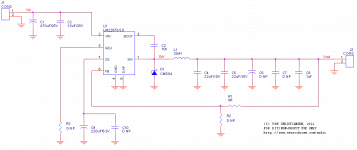
I've been playing with WebBench quite a bit lately. It looks like I can hit the required output voltages and currents without making any modifications to the board aside from changing out the inductor, output cap, and feedback resistor(s). But as the filament voltages usually aren't changed on the fly, I'm thinking that's an acceptable solution.
Attached is the schematic as well as the first stab at component placement on the PCB. Some routing required... 🙂
~Tom
Attachments
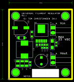
Tom, If you shift all the components to the right slightly you will improve the spacing between the two left screw holes and components. It looks like there is plenty of room to do so.
Tom, If you shift all the components to the right slightly you will improve the spacing between the two left screw holes and components. It looks like there is plenty of room to do so.
Yeah, I was mulling over that. J1, J2 are right-angle connectors and like to sit far from the board edges. I suppose, I could let them hang outside the board by a few mm... I need to get my paws on a handful of connectors and see how they work out in real life.
I am a bit concerned by the stresses from the mounting holes -- especially on the ceramic caps.
~Tom
On the other hand you might shift C4,5,7 right and move C8 all the way to the left of them to achieve some clearance there. Rotate D1 90 CW and shift left of C1, L1 and bring C1 down and you might have plenty of clearance.
Those are good points. -- Especially rotating D1, C1 and tightening up the C2-U1-D1 loop would be a welcome optimization.
~Tom
~Tom
You could also reverse the terminals on J1 to help routing, but it would leave one connector with the opposite polarity wrt the other. Minor for a multilayer board.
I prefer to have the polarities match. Part of that is my general neurotic state. But part of it is also ease of assembly or ease of use. It's bad enough that they're both 2-pin connectors. Someone will eventually hook the DC in from the rectifier to Vout...
With a ground plane on both sides, the (-) connection to Vin is easy. The (+) connection will be a tad long -- especially if C1 is rotated -- but with an 80-mil trace it really shouldn't matter much.
Another suggestion that's come up, is to bring out pins 5 and 7 to a header. This would allow for all the various LM2267x options to be used. Pins 5, 7 are used for current limiting, sync, enable, and other stuff depending on options. They all require a 0805 (or similar) component to GND, so they could share the same layout. That's an option under consideration anyway. It's not really relevant for my particular build, but would allow for more flexibility when using the board in other applications.
~Tom
Last edited:
After some mucking around...
Top layer + top silk shown. Bottom layer is a solid plane (aside from the holes for the output cap, connectors, and thermal vias of course). The top and bottom layers are stitched together with some via matrices (79 vias total).
~Tom
Top layer + top silk shown. Bottom layer is a solid plane (aside from the holes for the output cap, connectors, and thermal vias of course). The top and bottom layers are stitched together with some via matrices (79 vias total).
~Tom
Attachments
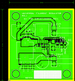
I think I'll include an option for using an SMD 6 or 8 mm electrolytic can for Cout. I'll let its footprint overlap with the existing through-hole Cout so it shouldn't blow up the board layout.
~Tom
~Tom
- Home
- Vendor's Bazaar
- Universal filament regulator