I'm not sure why you brought that up.
I am aware that the 2N3904 and ZTX831, for example, have different VAF, with the ZTX superior- roughly a 2:1 ratio if I remember correctly.
However, that is not an issue in this configuration, at least as far as small signal evaluation is concerned.
Here are the PSRR numbers vs frequency for the buffer in MC mode with 2N3904s and ZTX851s, measured at the output port.

The two cases almost overlap for the positive supply. And for the negative...

This is for a gain of 46dB.
I am aware that the 2N3904 and ZTX831, for example, have different VAF, with the ZTX superior- roughly a 2:1 ratio if I remember correctly.
However, that is not an issue in this configuration, at least as far as small signal evaluation is concerned.
Here are the PSRR numbers vs frequency for the buffer in MC mode with 2N3904s and ZTX851s, measured at the output port.
The two cases almost overlap for the positive supply. And for the negative...
This is for a gain of 46dB.
Last edited:
It's yet another reminder that SPICE simulations aren't "measurements" and SPICE transistor models often don't reflect reality.
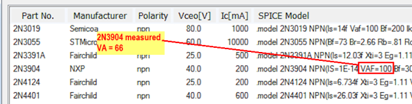
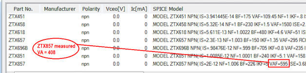
When I extract the slopes from the measured electrical data in #240 I find that at Ice=12mA, 2N3904 has an ro of 5500 ohms, corresponding to VA=66. I also find that at Ice=12mA, ZTX857 has an ro of 34K ohms, corresponding to VA=408. The ratio of these two Early voltages is 6.2 in the real (non SPICE) world. At least for the sample devices laying on my bench.
Curve tracer measurements have corrected faulty human intuition; the faults were caused by SPICE models not matching reality.
_
Attachments
Fine, but that makes little practical difference in this case., and there is no way to realistically incorporate this understanding in the present simulation environment.
In case you didn't know I spent considerable time at ADI working with the CAD group on the modelling (and device optimization) of complementary bipolar devices, including obscure issues such as quasi saturation, and later on in deep sub micron cmos where sub threshold issues were of extreme importance.
I am aware of the limitations of models, but I also know that prototyping (or silicon) is the ultimate arbiter and in the absence of a modelling group at my beck and call all I can do is use what is available and try to design around the limitations that LTspice imposes.
That's why I do prototypes. That's why I characterize them extensively. However, I will say that the avoidance of obvious errors is more important than being overly anxious about what often turn out to be second or third order effects.
I tell you what, I'll edit the models to reflect, at least to a first order, the VAF that you specify and see what happens....
So, the 3904 has a VAF of 66 and the ZTX851 has a VAF of 400. The end result is that the max positive PSRR dropped by 3dB for the 3904 and increased by 10dB for the ZTX851. The negative was essentially unchanged.
These changes occurred at frequencies of 300Hz and above, and in fact the negative PSRR still dominates.
I've returned the models to their original state and will retain the choice of device that I made, mostly because of inventory and cost issues.
These changes occurred at frequencies of 300Hz and above, and in fact the negative PSRR still dominates.
I've returned the models to their original state and will retain the choice of device that I made, mostly because of inventory and cost issues.
Don't be in such a hurry to type. Don't bypass proofreading and double checking. I hope you realize that 1 does not equal 7.
I hope you realize that ZTX851 is a different transistor than ZTX857. Consult the website of Diodes Inc. if you want independent confirmation.
I hope you realize that ZTX851 is a different transistor than ZTX857. Consult the website of Diodes Inc. if you want independent confirmation.
Yes, of course I can read, yes of course I can tell the difference and I knew that the device you characterized- for whatever reason- was not the ZTX851, but I needed to demonstrate a point and I have models for the ZTX851 and not the 857- and you're right I am in a hurry.
I have more important matters to consider than an argument that is tantamount to trying to decide how many angels can dance on the head of a pin (at least then you have an upper bound based on the Planck length). The consequence in this case is de minimis and is easily calculated as such, and I simulate the effect on the overall noise performance by including a source in the supply equivalent to the regulator datasheet output noise and determining the net degradation in S/N ratio. Beyond that I see no reason to pursue the matter further.
I have more important matters to consider than an argument that is tantamount to trying to decide how many angels can dance on the head of a pin (at least then you have an upper bound based on the Planck length). The consequence in this case is de minimis and is easily calculated as such, and I simulate the effect on the overall noise performance by including a source in the supply equivalent to the regulator datasheet output noise and determining the net degradation in S/N ratio. Beyond that I see no reason to pursue the matter further.
In case anyone is interested here is the approach I take to model the effect of the PSRR relative to the +/-15v regulators.
The published nominal rms noise at the output of an LM7815 is 90uv over a bandwidth 0f 10Hz-100kHz.
A 5meg R produces 91uv over a 10-100k bandwidth.
So, a source is added to the supplies that injects that noise. I then simulate the noise at the output of the block of interest and compare against the noise without the noise source.
With the present design the 20-20kHz output noise degrades by approximately 1dB when the supply noise, on both supplies, is increased by a factor of 850.
I consider this to be adequate margin.

Incidentally, this is an approach that I've taken several times in the past with, apparently, excellent practical results.
The published nominal rms noise at the output of an LM7815 is 90uv over a bandwidth 0f 10Hz-100kHz.
A 5meg R produces 91uv over a 10-100k bandwidth.
So, a source is added to the supplies that injects that noise. I then simulate the noise at the output of the block of interest and compare against the noise without the noise source.
With the present design the 20-20kHz output noise degrades by approximately 1dB when the supply noise, on both supplies, is increased by a factor of 850.
I consider this to be adequate margin.
Incidentally, this is an approach that I've taken several times in the past with, apparently, excellent practical results.

Perhaps the negative PSRR is impacted by the ro of the 2N3906 (PNP transistor) connected to the negative rail, and that may explain why changing the 2N3904 SPICE model has no effect upon simulated PSRR-negrail.
Luckily the '06 has an even worse ro than the '04, so it's even easier to improve. Horowitz and Hill's tables in their 3rd Edition list alternate PNPs whose ro (measured by them, not copied as gospel from datasheets or simulations) is a factor of 5x higher, and my own sequence of measurements (link) unearthed PNP devices whose ro is a factor of 10x higher than the 2N3906's. Thus the PNP-ro may be a low hanging fruit. Or, depending on the relative costs of the base bypass capacitors C8,C9 compared to the filtration PNP Q2, it might be cheaper to connect two complete copies of the filtration circuit block in series, then rejigger R18.
Luckily the '06 has an even worse ro than the '04, so it's even easier to improve. Horowitz and Hill's tables in their 3rd Edition list alternate PNPs whose ro (measured by them, not copied as gospel from datasheets or simulations) is a factor of 5x higher, and my own sequence of measurements (link) unearthed PNP devices whose ro is a factor of 10x higher than the 2N3906's. Thus the PNP-ro may be a low hanging fruit. Or, depending on the relative costs of the base bypass capacitors C8,C9 compared to the filtration PNP Q2, it might be cheaper to connect two complete copies of the filtration circuit block in series, then rejigger R18.
I think that it's just entirely inconsequential. Don't forget this design has a feedback factor of at least 50dB over the audio band.
This acts to increase the PSRR accordingly. Designs with lower feedback factor, say 15dB or so, will experience 35dB worse PS noise injection at the output for the same set of conditions. Again, the closed loop PSRR is high enough that the regulator induced output noise is in the order of 60dB below the input referenced noise and as such is inconsequential. Choosing transistors for a particular output characteristic seems, well, pointless. Choosing for cost, availability, adequacy and inventory control, seems more prudent.
If a different architecture were employed then this might not be the case, but this architecture has substantial merits- as long as you're not stuck on the idea that large amounts of negative feedback is bad.
My belief is - au contraire- large amounts of negative feedback- 50dB or more- is just fine and dandy and negates the assumed consequences of the use of negative feedback.
I chose 15dB as the reference as some evidence exists that, in some sense, 15dB negative feedback may be the worst level to adopt.
Well, as far as the negative rail PSRR is concerned, sometimes one just has to state the obvious, for completeness. I assume that you agree.
However, just for a test, even though you did not "correct" the early voltage for the 2N3906, I did change the 2N3906 in the same way as the 2N3904, again for completeness. The net result was that the PSRR degraded from about 72dB in the mid band to about 69dB. I also ran the overall PSRR noise test and the negative supply scaling to achieve 1dB degradation in output noise dropped to c. 600, if I remember correctly.
Again, this is a de minimis problem.
One of the several goals of this architectural approach is to greatly reduce the sensitivity to the supply- indeed below any reasonable expectation of effect.
Perhaps this is not true for low feedback, different architecture designs, but it is not the case here. I suspect that our 15dB negative feedback case, or an open loop case, would have a really hard time achieving comparable performance and would require much improved supplies or complex supply networks.
I would expect their comparable supply noise scaling parameters to be in the tens, rather than the hundreds, depending on the output noise.
The actual answer is that, for "production" (and indeed this, or some derivative thereof, may actually become a real product) I will use whatever low cost NPNs and PNPs I can get or have in stock- not specifically the 3904 and 3906s- and make an assessment then as to their suitability. The main reason for selecting the 4s and 6s at this time is that they are used in a variety of locations (often in relay control blocks) in the "production designs" that I have been involved with and are therefore available at lost cost and without inventory issues.
Part of the goal in this design is to create something that has near 100% production yield while using a contract manufacturing house, and after thorough postproduction testing to exacting specs for RIAA compliance, noise and distortion.
Not your usual DIY goals I concur, but at the same time it should, as a consequence, be a design that ports well to the needs of the DIY community in its DIY form.
Frankly, I think that this dead horse has been thoroughly beaten.
I'm in and out today, and I've been responding in small windows of time. The bulk of my day from now on is fully booked, so don't expect any near time responses, should a follow up post occur.
Sure. But It'll be a while. I've just completed the Kicad schematic, but the actual layout is new to me and is barely started. As an analog/mixed signal IC design engineer, I rarely had a reason to do my own layouts, and others have done my PC layouts since retirement and I'm still coming up to speed.
I'll post the "final" schematics, excluding the remote control digital "stuff", shortly.
I'll post the "final" schematics, excluding the remote control digital "stuff", shortly.
Some simulated results for the buffer/RIAA stage.

Nominal RIAA compliance 20Hz-20kHz. 5mdB p-p. 100mdB p-p max with 1% caps and 0.1% Rs in the RIAA stage.

Buffer Feedback factor for a 46dB (MC mode) closed loop gain - not open loop gain. This is the gain that is applied for correction.

As above, but with 26dB gain- MM mode.
Nominal RIAA compliance 20Hz-20kHz. 5mdB p-p. 100mdB p-p max with 1% caps and 0.1% Rs in the RIAA stage.
Buffer Feedback factor for a 46dB (MC mode) closed loop gain - not open loop gain. This is the gain that is applied for correction.
As above, but with 26dB gain- MM mode.
It looks excellent, I’ll have a closer look later. Is this designed as a standalone phono stage (rather than preamp input/volume functions)? I see the convenient selectable gain near the output stage.
Best wishes.
Best wishes.
Unlike its predecessor it's not immediately usable as a line stage as well as a stand alone phono stage., even if it does have limited balance (+/-3.4dB) and mono functions. It can be used in 2dB gain increments from 35dB to 73 dB, but the relationship is not straight forward.
In the case of an MC cart, if the input coupling C is 0.22uF, the impedance (real part) seen from the FET gate will be 510kΩ dominant in the low range, and noise will increase. I think it need at least a few tens of uF.

Thank you for the question and the interest.
Yes, the "1/f noise" (yes, I know it's not actually 1/f) will increase. However, the effect on the A weighted noise is minimal.
The small cap is beneficial because of the dynamics of the calibration loop. The resistors and the cap can be scaled, but no more than about a factor of 5 as the input impedance that I actually would prefer is c. 100k at 1kHz, due to the MM cartridge needs.
The unweighted 20-20kHz output noise after the RIAA stage is 445.6uv simulated, while the A weighted value is 40.7uv. The total gain is 61dB at 1kHz.
However, perhaps somewhat counter intuitively, depending on your intuition, if I do scale the impedances to 100k/500k with a 1u cap then the simulated integrated A-weighted noise actually worsens to 42.8uv- 0.4dB worse!
Below is the original circuit output A weighted noise.

Below is with the Cx5 and the Rs/5.
Note the increased LF "hump".

Just for interest sake- let's keep the Rs constant and increase the cap to 10uF. Something that is, well, impractical in this architecture because of the very slow rate at which the input calibration loop settles and the effect it has on the rest of the DC coupled amplifier stages.
The A-weighted output noise decreases to 37.9uv, a 0.6dB improvement!

Overall, I believe that the tradeoffs are, from an acoustic perspective, quite reasonable.
Yes, the "1/f noise" (yes, I know it's not actually 1/f) will increase. However, the effect on the A weighted noise is minimal.
The small cap is beneficial because of the dynamics of the calibration loop. The resistors and the cap can be scaled, but no more than about a factor of 5 as the input impedance that I actually would prefer is c. 100k at 1kHz, due to the MM cartridge needs.
The unweighted 20-20kHz output noise after the RIAA stage is 445.6uv simulated, while the A weighted value is 40.7uv. The total gain is 61dB at 1kHz.
However, perhaps somewhat counter intuitively, depending on your intuition, if I do scale the impedances to 100k/500k with a 1u cap then the simulated integrated A-weighted noise actually worsens to 42.8uv- 0.4dB worse!
Below is the original circuit output A weighted noise.
Below is with the Cx5 and the Rs/5.
Note the increased LF "hump".
Just for interest sake- let's keep the Rs constant and increase the cap to 10uF. Something that is, well, impractical in this architecture because of the very slow rate at which the input calibration loop settles and the effect it has on the rest of the DC coupled amplifier stages.
The A-weighted output noise decreases to 37.9uv, a 0.6dB improvement!
Overall, I believe that the tradeoffs are, from an acoustic perspective, quite reasonable.
Last edited:
To continue, now that dinner is over.
The Rs can be kept the same and the C can be increased to 0.47uF in simulation. This makes the A weighted RIAA noise look more "white", at least up until 2kHz or so, and reduces the integrated noise to 38.5uv, only a tenth of a dB or so worse than the 10uF case. The calibration takes proportionally longer, but the output DC offset loop may just take care of that. I can't simulate the effect of the output loop in a way that can achieve a conclusion, so the end result will be that I will test various input caps when I have the prototypes and see what is best, even if I'm not expecting the end result to be much different from what it is now.
The Rs can be kept the same and the C can be increased to 0.47uF in simulation. This makes the A weighted RIAA noise look more "white", at least up until 2kHz or so, and reduces the integrated noise to 38.5uv, only a tenth of a dB or so worse than the 10uF case. The calibration takes proportionally longer, but the output DC offset loop may just take care of that. I can't simulate the effect of the output loop in a way that can achieve a conclusion, so the end result will be that I will test various input caps when I have the prototypes and see what is best, even if I'm not expecting the end result to be much different from what it is now.
Thank you for answering.
Low-frequency noise is only a small difference in area when the frequency is on a linear scale, so I expected that the difference would not be that big with A weight.
I also checked, and was able to confirm that the difference was only a few tenths of a dB. I happened to have a FET input (k147/J72) MC phono amplifier board that I had made in the past on my bench, so I actually changed the gate resistance to 470kΩ and added a 0.22uF coupling to confirm it. I felt that there was no big difference in the audibility, nor in the woofer's shaking outside the audible range, which was a concern.
We apologize for the inconvenience. I also feel that I had a good experience.
Last edited:
- Home
- Source & Line
- Analogue Source
- Ultra high spec opamp MC/MM phono, warp "elliptic" filter, line, headphone amps