Unclear. Sean is commencing the buffer layout, I believe. I have to determine the best overall v4 configuration as it will have switches for loading, gain and will have SE/ group delay balanced outputs as well as the improved warp filter , input buffer etc. etc.
It only lacks a balanced input, and that I don't see the point of.
It's an easy thing to design and simulate, but a hard thing to layout and build, so kudos to Sean for doing it so expertly.
It only lacks a balanced input, and that I don't see the point of.
It's an easy thing to design and simulate, but a hard thing to layout and build, so kudos to Sean for doing it so expertly.
Yes, the v3.2 had almost all the desirable features that it could have. V4.0 will have them all (until the next input says, why don't you...)
Understood, Many thanks!Unclear. Sean is commencing the buffer layout, I believe. I have to determine the best overall v4 configuration as it will have switches for loading, gain and will have SE/ group delay balanced outputs as well as the improved warp filter , input buffer etc. etc.
It only lacks a balanced input, and that I don't see the point of.
It's an easy thing to design and simulate, but a hard thing to layout and build, so kudos to Sean for doing it so expertly.
The most recent schematic. It is being layed out, but that will take a while. The MC buffer parts are here, and the boards should arrive in a few days.
If it works as simulated, then the v4 will proceed. The 18v 1A AC wall wart is from Jameco and cheap.
No provision for a headphone amp is included.
If it works as simulated, then the v4 will proceed. The 18v 1A AC wall wart is from Jameco and cheap.
No provision for a headphone amp is included.
Attachments

Exciting developments on the front end, Wyn. The relay function switching for the elliptical warp filter and other functions is also a nice addition.
In any case, buckle up and brace yourselves. It’s about to kick in.

In any case, buckle up and brace yourselves. It’s about to kick in.
There's also a balanced "option" for the MC. It's intended for the circumstance that the SE version doesn't pan out as the design is dependent on the ZTX PNP and NPN having vbe's within about +/- 60mv of each other. If that is not the case the balanced design remains DC coupled with the same gain and a 2dB or so degradation in S/N ratio.
Attachments
The latest update. The intention now is to add a remote control option. All the gain switching is now relay controlled as well as the other functions except for input load in order to facilitate remote operation. A simple ATmega328 circuit will be used. The relay controls should be compatible with mechanical switches or the ATmega's outputs.
Attachments
More changes of intent. I've received quite a bit of feedback, and the goal now is to produce a "unified" MC/MM stage. That is, a single channel with FET inputs that meets the noise and gain requirements for MM and MC, with a gain range that can be stepped between 35dB and 73dB with 2dB resolution.
The input selection can be made prior to the input buffer so multiple channels can be selected.
The 46dB gain balanced MC stage was prototyped and works well.
The new SE FET input has about as low noise as the SE bipolar input (ignoring 1/f, but A weighted results are very close) and uses dynamic "calibration" of three sets of matched FET pairs (TI JFE2140) to avoid the need for FET selection.
It can be switched from 46dB (MC) to 26dB (MM).
Again, any questions, suggestions, observations are most welcome.
Attachments
I suggest you take a look at the Pearl 3 schematics by Wayne Colburn. Wayne is the Pass Labs fulltime employee who designs ALL of their preamp products.Again, any questions, suggestions, observations are most welcome.
(link) Pearl 3 Burning Amp 2023
It was unveiled three months ago at Burning Amp in Petaluma. Pearl 3 is a unified MC/MM phonostage with selectable gain and selectable cartridge loading. Input is 4 parallel (ballasted) Toshiba JFETs (current production devices), giving both low current noise density and low voltage noise density. The diyAudio Store {link at bottom of this Forum page} sells kits-of-all-parts including PCBs.
Those JFETs cost USD 0.39 per piece, which compares favorably to the USD 3.31 cost per piece for the JFE2140.
There are also a few community-designed remote power supplies for Pearl 3, to be housed in their own chassis, physically located some distance away, and connected to Pearl 3 by an umbilical cord. The most excessive kill-a-mosquito-with-a-bazooka example of this genre, goes by the name "UDP3" (Umbilical cable Driver for Pearl 3). Forum search will find it. Of course, many Pearl 3 builders will choose to put their power supply in the same chassis as the phonostage, and forget about multi chassis implementations with umbilicals.
Last edited:
Thanks.
I had not seen the Pearl 3 schematic before, but it was trivial to construct and simulate and make comparisons.
Despite some superficial similarities the operation of the proposed circuit is quite different to the Pearl 3.
The crudely calculated equivalent noise resistance is (70/2+11)/3=15 ohms for a start. The Vgs for the 2140 FETs varies from -1.1 to -0.5 even if the pairs are matched to within 4mv, so a calibration circuit is required to avoid matching via. a selection process.
The simulated A-weighted noise is also 6dB worse for the Pearl 3 than the proposed design.
The circuit operates as a transimpedance design, so the effective negative feedback level in the audio band is generally somewhat larger than the Pearl 3. This may not seem important to you, but it is vital to me.
For example, the "voltage gain" (from the inverting input gain to the output of the transimpedance stage) is 113dB at 1kHz and the "loop gain" (i.e. the feedback factor) is 64dB at 1kHz and, I believe, 45dB at 20kHz.
Simulations of the Pearl 3 indicate that the overall equivalent loop gain is 32+33dB=65dB (hand calculation and simulation agree), ignoring the "current sharing" at the low impedance inverting input, and the actual loop gain/feedback factor for a gain of c. 46dB is only 14dB at 1kHz and 11dB at 20kHz.
There are many other questions that I have, but I don't want to delve too deeply into the circuit details at this time.
Some more comments. Replacing the TI matched FETs with "matched" LSK170Bs (with 10 ohm ballast R) essentially matches the TI FET performance within a dB or so. The idea here was to eliminate the need for any kind of user FET matching.
As the FET bias current is 2mA or so 10 ohms will only accommodate a small degree of mismatching. I have no idea if this is significant or not.
If matched LSK170s, even as pairs, are available, then clearly, they are a better choice, which in no way detracts from the architectural differences.
The "calibration" function forces the -ve input terminal of each input stage to be very close to signal ground, which allows for the bias currents of the FETs to be well controlled by the resistors to the negative supply as no significant DC current flows through the feedback network.
I am unable to find any tolerance information on Vgs over device spread or Vgs versus drain current for LSk170s.
Are you aware of such information?
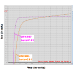
Also, what is the reason to choose ZTX831s for the NPNs. As far as I can determine a 2N3904 will perform just as well in those locations.
As the FET bias current is 2mA or so 10 ohms will only accommodate a small degree of mismatching. I have no idea if this is significant or not.
If matched LSK170s, even as pairs, are available, then clearly, they are a better choice, which in no way detracts from the architectural differences.
The "calibration" function forces the -ve input terminal of each input stage to be very close to signal ground, which allows for the bias currents of the FETs to be well controlled by the resistors to the negative supply as no significant DC current flows through the feedback network.
I am unable to find any tolerance information on Vgs over device spread or Vgs versus drain current for LSk170s.
Are you aware of such information?
Also, what is the reason to choose ZTX831s for the NPNs. As far as I can determine a 2N3904 will perform just as well in those locations.
The calibration matches a triplet of JFE2140s (or a sextuplet of JFE150s, which are the same FETs as singles) to within, effectively, +/-4mv, which translates out to IDSS variations of +/-100uv with a nominal IDSS of 2mA.
I see that matched (to +/-100uA) quad LSK170Bs are sold on DiyAudio for $30 and octets for c. 2x as much. That suggests that the calibration replaces $45 of FETs with $12 of FETs and $3 of components. This seems like a good deal to me.
I see that matched (to +/-100uA) quad LSK170Bs are sold on DiyAudio for $30 and octets for c. 2x as much. That suggests that the calibration replaces $45 of FETs with $12 of FETs and $3 of components. This seems like a good deal to me.
By the way is R10 on the Pearl3 schematic supposed to be 22k as drawn or 2k2? 2k2 seems to better match the operation and annotations. 22k would add about 22 ohms to the equivalent input noise resistance and would not give the drawn OL gain for the opamp stage in the input gain block. 2.2k would add about 2.5 ohms to the noise resistor. The 750 ohms adds about 0.8 ohms, degrading things by about 23 ohms as drawn or 3.3 ohms as surmised.
It would also increase the feedback factor by 20dB at 1kHz, bringing it up to a more acceptable, if still modest, number.
The use of the ZTX851s still remains a mystery as in both cases the base has a large effective resistance in series, so they can't be there for their "low noise", so is it for power handling?
After having Mark's actually very useful input on the FET choice- I've revisited the design and although the calibration remains, it now works with a single bank of 2SK209GRs. The calibration allows a wide range of FETs with IDSS of 3mA or above at Vgs=0 to be used without any possibility of internal operating point failure as the loop stabilizes the net bias current at c. 11ma, independent of the individual FET parameters- provided the minimum IDSS requirements are met.
A quintet of $.40c FETs is used per channel, operating at an average of 2.2mA each, which represents a c. sixfold reduction in total cost compared to the TI parts. No degeneration resistors are required if the above FETs are selected as the variation in IDSS and threshold lies within an acceptable range so that only minor changes in performance occur (according to simulations) with a mixed and matched set of worst-case devices (using my own models).
Relative to the TI based design the simulated results are about 2dB worse in S/N ratio.
The feedback factor for 46dB closed loop gain is 51dB or more over the entire audio band, peaking at 61dB at c. 1kHz.
If anyone is interested, I'll post the modified schematics.
Yes please. I love my WP phono—It gave me fast and direct access to playing about with MM carts again—and lots of chassis challenges with toggle switches etc, and a cool PSU implementation—WAY fun... it's in current rotation with Pearl 3 (with Mark's PSU offering) and Salas Ultra. Good company in my view—I'll be building any later variations you dream up....

Just the basic buffer/RIAA to begin with.
A very quick/superficial theory of operation.
It's a Transimpedance/current feedback buffer with an "active load", a loop that calibrates the multiple parallel FETs to c. 11mA total current, with enhanced "slew" current for the power up sequence, and an active I-V converter.
The "active" load increases the LF feedback factor and also helps to improve the LF open loop phase shift so that the LF closed loop frequency response peaking is controlled.
The output opamp is operated as an I-V converter-- which is why this is a transimpedance amplifier- so the output voltage is developed due to the signal current being transported through Q1 from the FET drains and into the virtual ground of U1. and through the feedback resistor R6.
The input impedance of the virtual ground is defined by the feedback R of 5.1meg divided by the frequency dependent gain of the opamp, so it looks like an inductor. Without the active load the frequency at which the signal current goes into the virtual ground drops due to current sharing with the load and the LF open loop gain drops, reducing the feedback factor with the potential to cause variations in frequency response and increased distortion.
The second stage is a conventional, but low closed loop gain and hence high feedback factor, RIAA stage, expected to have distortion in the -120dBc range at 20kHz. Nominal 20-20kHz RIAA accuracy simulates out to c. 6mdB p-p. Worst case <+/-50mdB with specified passives.
Simulated input noise level in MC mode (46dB gain input stage)- 37nv, A weighted 20Hz-20kHz. 613pv/rthz at 1kHz.
MM is a bit worse, due to R36 being in the circuit, but as the signal levels are 20dB larger it's inconsequential.
The calibration loop seeks to force the voltage at the sources of the FETs to ground. Thus, the gate voltage of the FETS will go to whatever is required to conduct the current through R18, setting the FET operating currents.
It takes about 20s for the DC operating points to settle down, so an output enable delay needs to be added.
The cascoding device (Q3) need not be anything fancy. The degradation in noise due to its presence is de minimis due to the relatively high output impedance of the FETs and the resulting high local feedback factor seen by the BJT.
The BJT also acts to minimize the Miller capacitance due to the FET Cgs reflected back to the input.
Q5 is turned off when the buffer is properly biased and plays no part in the operation.
A prototype with TI FETs works as expected and shows no pathologies that I could discern. Obviously, it needs to be demonstrated with the Toshiba FETs.
Any questions, observations?
Attachments
You might enjoy tinkering around with a transistor curve tracer and exploring device characteristics. Here for example are a pair of devices I had on my lab bench, a 2N3904 and a ZTX857. With a ruler and a calculator you can extract the hybrid-pi parameter "ro" = dVce/dIce and from that, compute the transistor "Early Voltage". It makes an important contribution to Power Supply Rejection Ratio.
(the plots are identical except one is zoomed-in more than the other)
_
(the plots are identical except one is zoomed-in more than the other)
_
Attachments

- Home
- Source & Line
- Analogue Source
- Ultra high spec opamp MC/MM phono, warp "elliptic" filter, line, headphone amps