I've not finished with the design for the boost converter just yet - the proposed components aren't being modelled, I'll invest more time pulling this together once I have proved 'in-theory' the concept could work. (In-practice could be something else)
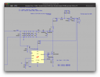
I've put the values of the main inductor from a coil craft that would fit the bill. I still have some noise reduction to do and D3 (playing with varactors) will be replaced by a safety should the high voltage diodes fail and conduct causing the rail to go HV. I've also got some tuning in terms of capacitance - that's simply a brute force approach but I wanted to test the boost with a large cap load.
I've got the supply set to provide 230V and current limiting to about 6A or there abouts simply to attempt to target 300W. In theory the RC oscillator control could be more active but it makes it easier to understand what is going on without it.
Currently running a full load test (see if the system sags) and then I'll run a 0V signal test to see if the system starts blanking pulses.
So this is looking good, this is with a 3.16V input on both channels (again one 10KHz, one 30Hz):
At the tube - front (green - cathode connected) and output (blue). Could do with dropping the B+ a little more but that's good.
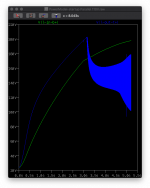
at the 24V PSU input - this is looking very good, doesn't seem to have any problem supporting the current required.
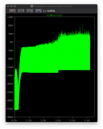
Output Tube looking ok (still needs some tuning but it's good enough for this step)

The output looks good so far.
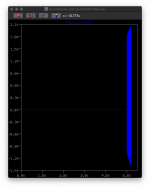
So in short this looks good. Next step is to lets this work through for a few seconds to see the noise level, then the next model will be zero input signal to see if the power draw drops too low and final noise model.
At the tube - front (green - cathode connected) and output (blue). Could do with dropping the B+ a little more but that's good.

at the 24V PSU input - this is looking very good, doesn't seem to have any problem supporting the current required.

Output Tube looking ok (still needs some tuning but it's good enough for this step)

The output looks good so far.

So in short this looks good. Next step is to lets this work through for a few seconds to see the noise level, then the next model will be zero input signal to see if the power draw drops too low and final noise model.
0V input signal to see how the power supply would behave. They say a picture is worth 1000 words:
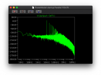
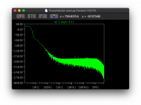
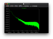
Output FFT 8-10secs on the simulation, so after the startup and in normal operation - note the low end noise <100Hz:
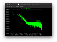
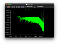
There's only one place that noise can come from in the system, so just FFTing the voltage source - switching noise.
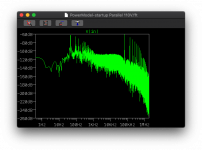
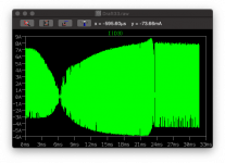
Looking at the current at this point - there's the source, blanking by the PWM chip to reduce the power:
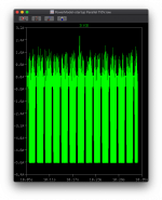
Hmm I need to look at the options of varying the oscillator to reduce power before the chip has to resort to blanking.
Output FFT 8-10secs on the simulation, so after the startup and in normal operation - note the low end noise <100Hz:

There's only one place that noise can come from in the system, so just FFTing the voltage source - switching noise.

Looking at the current at this point - there's the source, blanking by the PWM chip to reduce the power:

Hmm I need to look at the options of varying the oscillator to reduce power before the chip has to resort to blanking.
So in terms of solving the idle problem.
The problem is simple - when the system doesn't need power, switch off. That's what's happening with the blanking. It's using the lack of switching to reduce the power.
An alternative to reduce Q (the energy transferred) is to increase the frequency as the frequency increases, dI/dt is divided by a smaller amount. Given that devices become more inefficient (ie take longer to start the flow completely flowing) we can use that to become more inefficient.
The other alternative is to really have a hard filter or simply enable a switching bypass for blanked cycles to simply shunt a minimum current through a resistor. The idea of the shunt is to maintain the switching frequency that the load/filter, however thinking about it - the issue is that it's the gap in the current flowing through the diodes to result in the problem.
Reading through the LT site, the LT1243 is a 500KHz piece (not what the document states or infers) and the LT1246 is a 1Mhz piece with the same architecture. So I've switched to the LT1246 to see if this provide better resolution. Although the initial design probably won't support load properly the idea is to find a solution to the idle problem using a feedback based slope adjustment.
That would be the efficient way - an alternative is simply put a leak resistance to ensure a minimum power demand - perhaps even varying it based on the FB value.
If the FB value is within a % of the 2.5V point, it starts to open the current flow out of the filter. At 2.5V it would then be fully open and allowing the resistor then to dictate the minimum load.
The smoothing of the caps would then act to reduce noise or oscillation and if the amp needs power, then it would simply shut off. An alternative is making a mechanism with a minimal current flow (akin to a current limiter but current minim'er of you will) that simply skim off current however that's probably going to be a very hot and inefficient way. Let's see what the PSU switching changes results in.
Last edited:
This gives a nice summary and working for IMAX chips, these are similar to the LT/TI but the main things is it gives a nice explanation: https://pdfserv.maximintegrated.com/en/an/AN5587.pdf
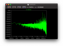
Initial run with feedback-based slope compensation.
Above is the is the oscillator, so it looks like I'm still getting sub-harmonics below 20KHz so I'll work through the maths later and see what I can do to reduce these.
The after that it's what can be done to supplement that if the voltage increases, how can we make the system less efficient without adding sub-harmonics to prevent the system from blanking and creating even more audible noise.
The filtered output seems to be cleaner though. This is full sim using just a non-loaded output - including the 6mF 1st order, so this really is the worse case for slow switching:
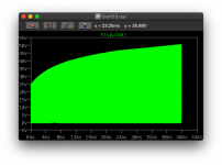
What the 24V psu would see:
As the LT1246 is a 100% duty capable at 1MHz it needs slope compensation and benefits from the capacitance to prevent oscillation and reduce sub-harmonics that become a problem with duty cycles over 50%.
I found a second interesting guide on this: https://www.ti.com/lit/an/slua837/slua837.pdf
Last edited:
Assumption efficiency = 70%
EQ1
Iin(avg,min) = Vout * Ioutmin / Vinmax * efficiency
230.0 * 0.100 / 24.0 * 0.70
Iin(avg,min) = 0.6708
EQ2
Iin(avg,max) = Vout * Ioutmax / Vinmax * efficiency
230.0 * 0.700 / 24.0 * 0.70
Iin(avg,max) = 4.6958
EQ3
Dmin = (Vout+Vd-Vinmax) / (Vout+Vd - ((Rds(on)+Rsense)*In(avg,min)
(230+1.2-24.15) / (230+1.2+((0.0050+0.0075)*0.6708)
Dmin = 207.05 / 231.2084 = 0.8952
EQ4
Dmax = (Vout+Vd-Vinmin) / (Vout+Vd - ((Rds(on)+Rsense)*In(avg,max)
(230+1.2-23.85) / (230+1.2+((0.0050+0.0075)*4.6958)
Dmax = 207.35 / 231.2587 = 0.8966
Duty range 89.5% to 89.7%
Note - Rds(on) and Rsense heavily impact the Duty range so keep as small as possible.
EQ5 - Given a 1Mhz switching frequency:
L >= Lc = 0.5*efficiency*(Vout+Vd)*D*(1-D)^2 / (fsw*Iout)
Lc(min duty) = 0.5*0.7*(200+1.2)*0.8952*(1-0.8952)^2 / (1x10^6 * 0.1)
= 0.69237 / 100000 = 0.0000069237 = 6.9237*10^-5 = 6.9237mH
Lc(max duty) = 0.5*0.7*(200+1.2)* 0.8966*(1-0.8966)^2 / (1x10^6 * 0.7)
= 0.67505 / 100000 = 0.0000067505 = 6.7505*10^-5 = 6.7505mH
L > than the 7mH minimum required
EQ6 & EQ7
LIR = ILpp / Iin(avg)
Iin(avg) = Iin(avg,min)+(Iin(avg,max)-Iin(avg,min))/2 = 0.6708 + (4.6958-0.6708)/2 = 2.6833 A
LIR = (Vout+Vd-Vin)*(1-D) / (fsw*L*In(avg)
= (200+1.2-24)*(1-0.8952) / (1*10^6 * 7.0*10^-4 * 2.6833) = 18.5706 / 1878.31 = 0.009886
LIR range 0.3-0.5. Otherwise the inductor needs a higher ILpeak to minimise losses.
The above is with 70mH, however with 7mH we are simply 0.0x thus given the power required, we are being very lossy at this switching rate.
EQ8
ILpeak = Iin(avg)*(1+LIR/2) = 2.6833*(1+0.009886/2) = 2.6956 A
So this marries up with our very small peak-to-peak current swings seen in simulation.
EQ9
Assuming 6mV with a 100mV margin,
Rsense = 0.106 / 1.0*ILpeak = 0.106 / 2.6956 = 0.0393 or 39mOhm
EQ10 & EQ11
Target ripple is 1mV
Cout > Ioutmax * Dmax / 0.5*Voutripple * fsw = 0.7* 0.8966 / 0.5*0.001*10^6 = 0.001255 F = 1.2mF
Thus if we use a 5.1ohm + 6*1mF to give a 0.5Hz LPF we’re good.
ESRout < 0.5*Voutripple / Ioutmax = 0.5*0.001/0.7 = 0.0007142, ESR < 0.7mOhm
Thus we can see ESR impacts our voltage ripple, thus paralleling output caps reduces ESR. With 6 caps in parallel 1/0.7m = 6*(1/esr) means 1400.168 = 6/esr, thus esr per cap = 0.004285 or below 4.2852 mOhm each.
Incidentally the ESR on 1mF 450 caps can range from 60-160+ mOhms. Low ESR caps are in the 60-80mOhm range for this sized cap. Smaller caps such as 450V 470uF are in the 120mOhm area. However large caps can give better ESR, a 4700uF 450V cap gives 14mOhm each but then you have more heating effect with less cooling surface area and higher current per cap.
SLOPE COMPENSATION
I detect frequency domain and complex maths here.. so going to get a coffee..
EQ12
A(f) = ACM * ((1+j*f/fzesr)*(1-j*f/fzrhp)) / (1+j*t/tpload) * (1+f/pi*Q*fsw+f^2/pi^2*fsw^2)
EQ13
ACM = (1-D) * Rload / 2*Rsense*CSgain
EQ14
fzesr = 1 / 2*pi*Cout*Resr
EQ15
fzrhp = Rload*(Vin/Vout)^2 / 2*pi*L
EQ16
fpload = 1/ pi*Cout*Rload
EQ17
B(f) = AFB * AEA * (1+j*f/fzea) / (1+j*f/fpea)*(1+j*f/fp2ea))
EQ18
AFB = Vref/Vout
EQ19
AEA = gm*Rout
EQ20
fzea = 1 / 2*pi*Ccomp*Rcomp
EQ21
fpea = 1 / 2*pi*Ccomp*(Rout+Rcomp)
EQ22
fp2ea = 1 / 2*pi*Ccomp2*(Rcomp||Rout)
EQ23
Loop(f) = A(f) * B(f)
EQ24
Q = 1/ pi*((1-D)*Se/Sn+0.5-D)
EQ25
Sn = Vin/L * Rsense
EQ26
Se = Icomp * (Rslope + Rsense) where Icomp = the chip comp current
EQ27
Rslope = (1/pi + Dmax-0.5) * Vinmin * Rsense / (1-Dmax)*Icomp(min)*fsw*L - Rsense
So there are 56 equations in this design sequence.. but I need coffee and breakfast.
Last edited:
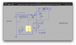
So I switched to a NTHL060N090SC1, a 900V 46A 60mOhm mosfet.
https://www.mouser.co.uk/datasheet/2/308/NTHL060N090SC1_D-1698980.pdf
The model is encrypted, but it seems considerably more finicky about the setup. It's also especially sensitive to transient noise causing the model to stop with a time step too small if steps aren't taken to reduce the interference. R11 is a simple load.
So changes:
* switch Cinput to 300uF low esr 63V Panasonic caps in parallel, same as C3. They're cheap but also very good esr for the size. This area should only have 24V but I'll put a 25V diode so if the system has a safety on shutdown (the inductor energy has to to somewhere).
* snubber on the input R10+C10 to help reduce noise cycling back to the Vcc pin
* non-dispersant resonator snubber on L1 - this recycles the spikes back by storing in C11 rather than just shunting to ground. This is sub-optimal at the moment as I'm using a second L1 essentially to make a mirror.
* U2 is the new mosfet - this is a fast fet, so caused me an absolute nightmare initially. You'll note the small gate resistor and D7.
* tail snubber R12+C12 to take the switch spike off the Isense.
* Q1+R8+R9 are a current slope compensation. This is mandatory as we can run 100% duty cycle on this chip and shapes the size of the pulse dynamically. If more power is needed then then you'll see a flat topped square wave, when the demand is less this becomes a slope from bottom to top as a sawtooth.
This dynamic makes filtering a little hard when it decides to reduce the output to a minimal amount- I think that's what may be causing the instability.
* timing R5+C4 is setup for about 40Khz at the moment, you can ramp this up and the mosfet will take it but be prepared to go through a re-specify the current filters in place.
The model is current have a longer run and I can already see some DefCon 1 appearing. So it's not entirely stable at the moment.
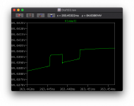
This is the only noise I'm getting out of it at the moment:
Last edited:
I found this On Semi document going over design aspects and different SMPS topologies. Worth a look if you're interested: https://www.onsemi.com/pub/Collateral/SMPSRM-D.PDF
In short - one aspect of that document is that it defines this PSU almost on the bounds of boost and half-bridge topologies. Many as the Boost topology needs at least 2xVout support from the mosfet and components. Whereas the Half-bridge and later full bridge only need Vin. The down side is that they have a transformer and bridge rectifier in the middle but can deliver more power.
The limitations appear in large boost converters - to get speed, you need low capacitance gates etc plus you want low impedance to handle the current without causing too much thermal output. So in short you're probably limited to 300-400V at which point the mosfet would need 900-1.2kV and the gates start needing more current to drive (higher capacitance).
In other news.. the new power supply is current sat running on the big amp model.. slow but let's see what comes of it 🙂
Last edited:
So the new mosfet is exceptionally quick, so quick that it will pick up ringing noise returning through the Vcc supply and act on it as it comes out of the output drive for the mosfet!
So I'm now running to 630KHz and it seems stable, I won't know until it passes the full run..
So it's extremely important to implement ringing control - such as a 50mOhm+21n RC snubber to damp the initial ringing spike (switch off capacitance 25A spike at 34MHz was enough).
Other news - this is now running both the appropriate models for Coilcraft inductor, STTH fast switching diode, for slope compensation NPN and mosfet.
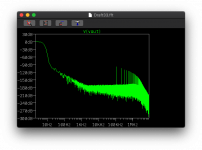
With the switching frequency set to ~100Khz it seems clean, the main question is - will it allow the boost to get to 230V? Still waiting for it to get to 230V but this is without the slope compensation but it's ticking over.. with a light load. This means the Ton periods are very very small at the moment.
The lower the frequency the more efficient, but at the same time the harder it is to filter from the audio spectrum.
What I'm hoping for is that we can get a 100KHz boost converter that can do 200-300Vdc at decent current (ie 1A of needed and have the noise sit above 20Khz even when the system start blanking.
I found a cap over the 50uF inductor worked better than the non-dispersive snubber as it kept bypassing all the current pulses needed to get about 2x voltage output What is nice is the system, at the moment, seems completely stable..
Interestingly enough if you do the maths:
* low voltage to high voltage = high duty % which is very prone to instability.
* losses are scaled with switching frequency.
* higher specification of components (ie 2xVout)
ESR and Z of the input needs to be low hence the need for input capacitance that is paralleled and has low impedance.
So this probably explains why there are few boost converters going from 24V to 230V specially with more power.
I have some more ideas, the inductor I’m using is too small and switching frequency may need a little more dropping, I may also change the other components again to reduxe losses.
If that doesn’t work the I’m looking at half or full bridge converters.. which typically support over 200W upwards with less current and voltage requirements. The cost may be some additional ripple but..
I’ve not given up on the boost idea.
The frequency is driven by a saw tooth RC. The duty rate and frequency could be halted making it more efficient - but interleaved two boosts off the same RC.
This means each inductor and mosfet run at 50kHz giving time for the inductor to charge. Then pulse into the same cap bank.
The only issue is typically the lower frequency needs a larger inductor.
Worthy of an experimental sim.
So after playing a little.. I've figured out that the mosfet is bounding on the inrush current - is short 1A 18V gate drive causes it some problems, so I now have two resistors in a divider to drop the voltage to 8-9V this means that current switch isn't as harsh and the system is (within reason) behaving itself.
It's running at about 250KHz and it's now up to 98V.. although it's blowing a few Defcon 1 messages.. so I suspect there's hell to pay on the current spikes and EMI.
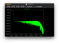
I'll leave it going .. it's just about stable..
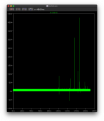
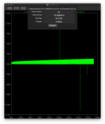
If that average is anything to go by, that's not bad..
It's running at about 250KHz and it's now up to 98V.. although it's blowing a few Defcon 1 messages.. so I suspect there's hell to pay on the current spikes and EMI.

I'll leave it going .. it's just about stable..


If that average is anything to go by, that's not bad..
Last edited:
So, I’m attempting to keep with continuous current mode (ccm) rather than dcm to keep the ripple and loss to a minimum. However I need to find a point where (a) the flux thus current is a good couple of amps, (b) the switch time is outside of the audio spectrum including sub harmonics etc and keeping reasonably efficient.
Only issue is that ccm is inverse (ie 1-duty cycle) to the due to the mosfet being on then switching off the pump current.
I’ve managed to make the chip more stable - looking at the block diagram the Vcc is input to both the gate drive and the vref that’s used for the oscillator sawtooth. So adding caps to the vref and the vcc pins has stabilised them no end.
So tomorrow I’ll have a look at getting 2A out of a 47uF inductor...
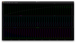
Timing graph for those interested.
Top pane - the voltage between the inductor and mosfet and diode. grey the output current from the LPF resistor in the output.
Middle the RC oscillator, cap and pin showing sawtooth.
Bottom - the inductor, mosfet gate and the Isense.
So back to the 47uH, I've tried nH too, but interesting here - as we go from CCM to DCM mode where the inductor bottom L1 is grounding out the current to 0mA - we start seeing a load of harmonics being generated in the green voltage between it and the switch (top green).
So if we can keep in CCM mode, the amount of harmonics should be less and we should have less noise.
So what I'm aiming for is a ccm with about a 5A-pp at the inductor within the 10A without either topping out or grounding out.
The Rsense provides max current but we need to shape the on waveform to manage the minimum drop. That way it should remain stable.
The Rsense provides max current but we need to shape the on waveform to manage the minimum drop. That way it should remain stable.
- Home
- Amplifiers
- Power Supplies
- Tube use? 24->300V large cap charger with 300V 150mA reg
