My initial attempt at a PCB layout - I've tried to keep the mosfet and the bio on the edge for heatsink attachment. I've then tried to keep the dI/dt loop as small as possible given the size of the inductors. The board has left quiet side, mid HV dI/dt noise and right side LV dI/dt. I've used the fact the mosfet and the diode has legs to jump a little. I still need to add the bypass and I may move the output caps to feedback onto the main ground.
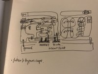
This morning I found this: SV1BSX's DC to DC Up Converter which has not a bad layout but given my inductors are 40x40mm each and the power needed is higher plus I don't like the long FB/sense runs under the mosfet (high dI/dt).
I've stolen a few ideas from this - and remodelled the B+ output lines making it shorter and existing mid board. This also allows the ground noise to remain on the noisy side of the board.
Last edited:
Loops affect performance. Specifically:
* dI/dt loops
* ground bounce loops
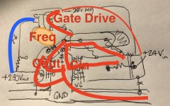
So back to first principles. Here's the current loops:
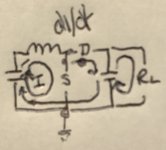
So in reality we have a circuit that's a star ground with components: This shows the smallest loops:
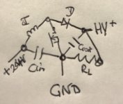
Next this got me going back to the drawing board and throwing away my initial design. Also throwing away the requirement for the mosfet and diodes to be on the edge of the board. Instead the design, like I've read on the LT and TI posts really focuses on minimising the high dI/dt loop areas and secondly looks at both grounds loop bounce (where the return current cuts the corner early making a larger loop area) plus look at making low impedance paths and not simply blindly relying on the ground plane.
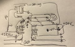
The heat sink now sits flat against the PCB on a standoff the mosfet and diode then sit with curved (not hard 90deg bends) to allow the loops to be closed in a tighter area. The bulky inductors caps and resistors will be sat on the opposite side so they're soldered through the board.
I still have some thinking/work todo - the but I can see the loops from Cin to mosfet and the mosefet to Cout are as small as humanly possible.
This design also frees up the gate pin on the mosfet - allowing the PWM controller IC (LT1243) to be positioned outside of the loops and also provides space to add a 24V regulator for Vcc plus.. the very noise sensitive FB is way way way from the noisy area.
* dI/dt loops
* ground bounce loops
So back to first principles. Here's the current loops:

So in reality we have a circuit that's a star ground with components: This shows the smallest loops:

Next this got me going back to the drawing board and throwing away my initial design. Also throwing away the requirement for the mosfet and diodes to be on the edge of the board. Instead the design, like I've read on the LT and TI posts really focuses on minimising the high dI/dt loop areas and secondly looks at both grounds loop bounce (where the return current cuts the corner early making a larger loop area) plus look at making low impedance paths and not simply blindly relying on the ground plane.

The heat sink now sits flat against the PCB on a standoff the mosfet and diode then sit with curved (not hard 90deg bends) to allow the loops to be closed in a tighter area. The bulky inductors caps and resistors will be sat on the opposite side so they're soldered through the board.
I still have some thinking/work todo - the but I can see the loops from Cin to mosfet and the mosefet to Cout are as small as humanly possible.
This design also frees up the gate pin on the mosfet - allowing the PWM controller IC (LT1243) to be positioned outside of the loops and also provides space to add a 24V regulator for Vcc plus.. the very noise sensitive FB is way way way from the noisy area.

Your analysis seems on point, you may want to add footprints for 5mm ceramic caps everywhere, and look into snubber design. But honestly i think right around 50-75Khz is the way to go, this produces less switching losses, and conduction losses should be mild, in the single digit watt range.
I suggest you look at the 2SK356X series of toshiba mosfets, Or the new Silicon carbide parts.
5A 900V devices, but these run well from the slow wimpy driver in the 3843.
Post filter should consist of something like 10uH 10uF followed by 1206SMD ferrite beads, once you find out what frequency the circuit makes FM at, you can add these filters to get rid of most if not all of it:
Protip, if you get a TL783 put a zener+ Optocoupler + resistor over the three terminal reg, you can build a nice adjustable supply with a switching pre-regulator.
Cheers,
V4lve.
Last edited:
I'm wondering if it's worth adding a 5.5mH common mode choke to target the SMPS residual noise.
lol just seen your post VL - thank you I'll look that that. Current switching is actually 57KHz so down a far bit from the 100Khz+. I started on the idea of a bead too but that needs tuning rather than modelling.
I've just been running through looking at the caps over the last couple of days. I think the timing RC as a C0G with the others being specifically low ESR (the 300uF Cin are 33mOhm and paralleled for example). Cout actually I have two - a WIMA DC Link 80uF to take the power from the diode, then a resistor and a 20uF to provide a little final ripple management both are 6mOhm.
I'll have a look at the other options for the 900V devices. I tried an infinion mosfet but their model seemed to have issues.
Last edited:
Just looked at Rohm instead of Inf etc, at their 1200V versions - SCT3040KL expensive but with a little adjustment and it's really making the PSU fly. I know the STM I had in the design had a 320mOhm but this is 40mOhm and 20A and it flies! (specL MOSFET 1200V 55A 262W SIC 40mOhm TO-247N - £34). I get the impression that it's a little overkill... just a slight amount 😀
Seriously it I suspect that the design could easily be scaled up with the appropriate adjustments.
Just keeping the 13A current limit and it's up to 250V 700mA. Let me see what this would do maxing out the inductors (14A for both).. 270V 750mA - pulling 14A through the inductors. Add more inductors and that goes up 🙂
Hmm model, with just under 20A limit is putting out 240V 1.2A.. into a 200ohm load (about 300W)..
Last edited:
What about this one?
Great progress by the way
C3M0280090D Wolfspeed(CREE) - Transistor: N-MOSFET | SiC; unipolair; 900V; 7,5A; 54W; TO247-3; 20ns | TME - Elektronische Componenten
Great progress by the way
C3M0280090D Wolfspeed(CREE) - Transistor: N-MOSFET | SiC; unipolair; 900V; 7,5A; 54W; TO247-3; 20ns | TME - Elektronische Componenten
Last edited:
I'll have a look in a bit.
I've had to adapt some of the models for the 4 pin WIMAs but it's all starting to appear in the PCB layout tool. I'm still working through finalising the BOM - there's a 2.4uF DC link I want to put in - that has an impedance dip that sits slap bang in the 50-100Khz region and really cleans up the simulation noise I'll probably put the foot print in for that.
I'm currently looking at sense resistors - bearing in mind that 24V at upto 14A. So this SOT 227-4 100W sense resistor I've currently got my eye on. 75mOhm means it's the right value for what I need: https://www.mouser.co.uk/datasheet/2/303/res_tghg-1265558.pdf I'll not be using the kelvin connection directly but it should be fine to ground
Not finished yet - the axis measurements are 240mm x 120mm.
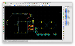
Caps and inductors on one side, components for the HS on the other.
I've had to adapt some of the models for the 4 pin WIMAs but it's all starting to appear in the PCB layout tool. I'm still working through finalising the BOM - there's a 2.4uF DC link I want to put in - that has an impedance dip that sits slap bang in the 50-100Khz region and really cleans up the simulation noise I'll probably put the foot print in for that.
I'm currently looking at sense resistors - bearing in mind that 24V at upto 14A. So this SOT 227-4 100W sense resistor I've currently got my eye on. 75mOhm means it's the right value for what I need: https://www.mouser.co.uk/datasheet/2/303/res_tghg-1265558.pdf I'll not be using the kelvin connection directly but it should be fine to ground
Not finished yet - the axis measurements are 240mm x 120mm.

Caps and inductors on one side, components for the HS on the other.
Still got a fair way to go..
Tried the 3D model for the first time hehe.. shows my footprints don't have the correct length update to the 3D model. Also the tracks are weedy just to stop my head exploding.. those will be removed and updated with a pour. Also there more work required.. far from complete. I can see some optimisations (like the TVS being connected to the fuse causing it to blow first not through the resistor) and some problems (R6 has it's back to the caps) also they should all be on the opposite side of the board so it may need some reorientation..
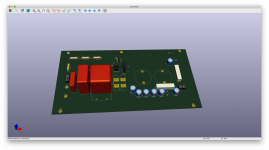

Tried the 3D model for the first time hehe.. shows my footprints don't have the correct length update to the 3D model. Also the tracks are weedy just to stop my head exploding.. those will be removed and updated with a pour. Also there more work required.. far from complete. I can see some optimisations (like the TVS being connected to the fuse causing it to blow first not through the resistor) and some problems (R6 has it's back to the caps) also they should all be on the opposite side of the board so it may need some reorientation..

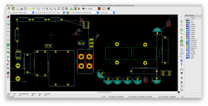
Found the flip command, so I can now demonstrate my plan:
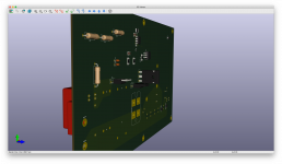
The idea is that the side you see will have heatsink(s) making a sandwich.
The other side, where it will be ground planed in the right places (the ground plane doesn't carry the current but simply acts as an EMI shield. The heatsink, grounded and sandwiching the diodes, mosfet and resistor, acts like the second EMI shield.
The two inductors are unshielded, so if I get EMI this is likely the main culprit. Also they will not have a ground plane underneath simply to ensure the ground plane doesn't suck the flux out of them.
I want to shave a little high off it - possibly to 10cm.
I still need to check the sense resistor pins vs orientation and a load of clearances to allow a HS to be mounted. One point is that the current sense line between the pins of the diode is probably pushing my luck with large HV spikes. That needs clearance so I may have to run a track on the opposite side (it's low voltage and low current).
Last edited:
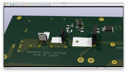
Now the question is - can you get 'left handed' diode packages, ie the cathode and anode are on the opposite pins?
Currently I'd like to bend the diode over so it sits in the diode space on the heatsink, however the pins are the wrong way around todo this. Anyone know if there's a standard to offer both? Currently I just see right handed..
Today's tasks are:
* I've already rotated the diode but ...
* Update track widths - 20 amps with 2oz copper and 40degC = 7.68mm track width, so the mosfet pin footprint needs adjusting as the standard footprint can't take that and maintain the spacing required for 900V. I'll also need to adjust the pin foot prints for the diode. The resistor should be fine given we're not pulling more than an amp but the clearances and creepage needs to be checked.
Remodeling the foot print - the TO-247 now has a space for 20A tracks with 5mm clearance between. Given we have a cap on one side and a inductor pair on the other we're going to get some spikes.
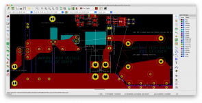
Just need todo the diode foot print.
I'm still weighing up if I should bother with a single heatsink or go separates - I'm trying to keep the devices on a vertical plane so a decent HS can convection cool.
The need for the wider tracks means I can't put a through access hole to mount a single HS and have it easily serviceable. Also the days of screws through into heatsinks are numbered (clips and silicone boot preferred) due to creepage at high voltage.
So still need to tidy up, but the tracks are now setup with net classes to ensure the correct track sizes, clearances etc for the current and voltages.
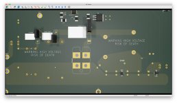
The spacings are a little OTT but now the system has 900V & 20A capable tracks through to the final resistor. That way it's not going have burnt PCB tracks through inrush.
Also put the sense resistor back- it's difficult to think which side is which but I think I have it correct. Not a biggie if not to switch.
Next up is clearing up the SMD and the IC, this really should perhaps be rotated to make it easier.
Now I've had a play taking the design to PCB, I'm looping back around to look at some finer tuning at full load (ie 600mA+).
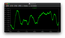
57KHz seems to give a stable but has about 20mV ripple whereas 75KHz has about 0.6mV frequency ripple (ie the switching) but I note that the voltage wanders. Here's the 75Khz with a 52mV wander:
The same exists for the 57KHz rate with a about 40mV wander:
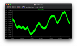
This looks like harmonics causing oscillation.
I'm about to look into snubbers again to see if that can be damped. The LT1243 actually has a blanking system so that the lead spike for the current sense ignores the first 100ns - which is long enough to cope with the mosfet switch. So I'm less worried about that.
I've also looked for the TI783 ltspice model but it appears non exists in the wild unless there's some hidden model I've not uncovered. My thinking here is that this would help the wandering considerably - given it has a regulation in the region of 0.001% with a zenner of 12V to float it, then we should be able to get 0.00012V regulation or 1.2mV.
57KHz seems to give a stable but has about 20mV ripple whereas 75KHz has about 0.6mV frequency ripple (ie the switching) but I note that the voltage wanders. Here's the 75Khz with a 52mV wander:

The same exists for the 57KHz rate with a about 40mV wander:

This looks like harmonics causing oscillation.
I'm about to look into snubbers again to see if that can be damped. The LT1243 actually has a blanking system so that the lead spike for the current sense ignores the first 100ns - which is long enough to cope with the mosfet switch. So I'm less worried about that.
I've also looked for the TI783 ltspice model but it appears non exists in the wild unless there's some hidden model I've not uncovered. My thinking here is that this would help the wandering considerably - given it has a regulation in the region of 0.001% with a zenner of 12V to float it, then we should be able to get 0.00012V regulation or 1.2mV.
Just to finish for the day.. for giggles.. 170ohm load..
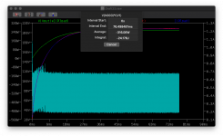
316W in .. 240W out..
That'd probably the max I'd want to shove through it given the inductors are running at 4W each, the diode is 1.3W and the mosfet is 17W (12A) at it's 13A current limiting. Also the output is getting a little ragged thus showing the lack of capacitance to cope with the current and ripple:

I have an idea for a more compact and less EMI radiating design.
The open core coils without shielding end up radiating a large amount of EMI, with copper cladding under them the flux thus performance falls supposedly and so I'm thinking of a design that minimises EMI and makes the dI/dt loops even smaller. Only down side is that it's using layers on top of each other to transport and cancel out the EMI from the main tracks. Then the issue becomes voltage vs board composition.
In my head I have the idea that the design will be a smaller board although the component sizes don't really change the spacing between them can be smaller.
So trying the 'deluxe' edition..
So first stop... switch out the PCV2 560uH unshielded inductor in favour of a 470uH shielded inductor that takes higher current - keeping the current limit at 13A.
I've added two more Cin caps as the lower resistance inductor was pushing each cap to 1.2A from their rated 1.5A, so with two more each cap is now 0.9A and the total ESR is even lower.
I've also added four 20uF WIMA caps in addition to take the power from the diode on each pulse. The reduced esr seemed to help no end..
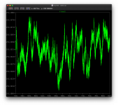
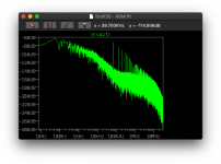
The above is providing 660mA at 250V. The above is showing the full ripple at about 7mV.. Add a post-supply regulator and you should be almost flat.. (did I say that the input has 150mVpp ripple added?)
Stress testing with 170ohm gave the same results (although slightly improved due to the added caps and the lower esr), and to be honest I'd expect the post regulator to lap that up (although 1.2A would kill the 783 for example).
Attached is the LTSpice model.
So first stop... switch out the PCV2 560uH unshielded inductor in favour of a 470uH shielded inductor that takes higher current - keeping the current limit at 13A.
I've added two more Cin caps as the lower resistance inductor was pushing each cap to 1.2A from their rated 1.5A, so with two more each cap is now 0.9A and the total ESR is even lower.
I've also added four 20uF WIMA caps in addition to take the power from the diode on each pulse. The reduced esr seemed to help no end..


The above is providing 660mA at 250V. The above is showing the full ripple at about 7mV.. Add a post-supply regulator and you should be almost flat.. (did I say that the input has 150mVpp ripple added?)
Stress testing with 170ohm gave the same results (although slightly improved due to the added caps and the lower esr), and to be honest I'd expect the post regulator to lap that up (although 1.2A would kill the 783 for example).
Attached is the LTSpice model.
Attachments
Last edited:
- Home
- Amplifiers
- Power Supplies
- Tube use? 24->300V large cap charger with 300V 150mA reg
