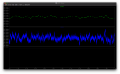
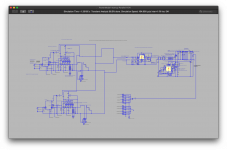
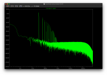
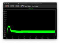
So.. Tracing back the noise - I can see that the Isense doesn't worry about the leading transient however the NPN does I believe. So I've added some snubbage 🙂
The output from the boost section is good and seems clean enough, the only variants in wave form is the variation from the PWM itself which is controlling the current but has an accumulative cycle and then decides it needs to have a fractionally larger gap - this occurs at 7KHz so it's easy to spot.
Now then..
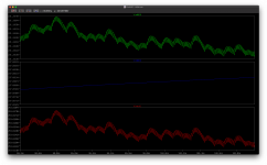
Top is output into the load. Middle is output from the maida mosfet... and the bottom is the output from the SMPS.
So it appears that currently the mosfet is setup to allow uA through.. which isn't enough to correct.. so the 600mA is going through the D1 diode as it keeps it 20V separation.. so a little more current is needed through the regulator 😀
Edit.. Turns out that that R1 is too large and that prevents the regulator from starting. The regulator is now starting up.. and the slow start should take about 900ms - the SMPS is already at 260V.. Let's see what happens after dinner 🙂
The output from the boost section is good and seems clean enough, the only variants in wave form is the variation from the PWM itself which is controlling the current but has an accumulative cycle and then decides it needs to have a fractionally larger gap - this occurs at 7KHz so it's easy to spot.
Now then..

Top is output into the load. Middle is output from the maida mosfet... and the bottom is the output from the SMPS.
So it appears that currently the mosfet is setup to allow uA through.. which isn't enough to correct.. so the 600mA is going through the D1 diode as it keeps it 20V separation.. so a little more current is needed through the regulator 😀
Edit.. Turns out that that R1 is too large and that prevents the regulator from starting. The regulator is now starting up.. and the slow start should take about 900ms - the SMPS is already at 260V.. Let's see what happens after dinner 🙂
Last edited:
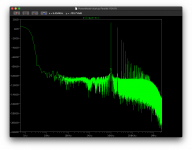
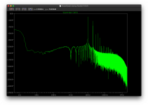
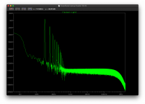
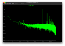
Ok last ones for today I suspect. 4.5 to 5.8 seconds:
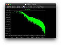
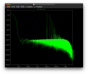
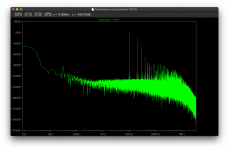
At the headset load 32ohm. Left channel 10Khz 3.16V input, right channel is 30Hz 3.16V:
Left
Right
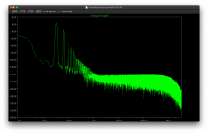
So apart from my amp's signal path not being anywhere near clean, the power supply (which I'm concerned with) looks very promising.
I still think the real value would be +20dB on that but until it's built you known nothing John Snow..
At the headset load 32ohm. Left channel 10Khz 3.16V input, right channel is 30Hz 3.16V:
Left

Right

So apart from my amp's signal path not being anywhere near clean, the power supply (which I'm concerned with) looks very promising.
I still think the real value would be +20dB on that but until it's built you known nothing John Snow..
Just thinking about/exploring ideas with using a parallel ground plane for the return. Early days but something even more compressed in terms of dI/dt loop - this is just to show the thinking:
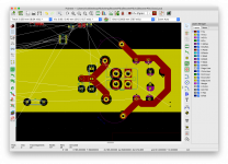
The concept is to have the top layer as HV and high current signal, the second layer (internal) as a large low impedance strip that provides an immediate return path. The third layer is a full second ground plane for shielding and the final back side layer being for feedback, sense (although I may route this in layer 3.
Note in the diagram I've still got the PCV2 footprint which is unshielded, but I would look to use a shielded inductor instead. Also think of the red tracks as some large fills instead. Some tidy up and clearances but these are currently set to 3.5mm clearance and the tracks are 7.68mm wide - enough for 20A with 2oz and only get a 40degC increase in temps.
To be honest this sounds like over kill with the SMPS PWM chip on the other side of the board. It would allow for quieter 24V signal but the switching from the chip itself will see a large amount of noise. So not sure if that would still be better on the main power side.
Last edited:
A better way of explaining it..
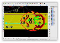
So the 24V high current supply comes in right (orange arrow), the Cin caps then provide the low ESR source feeding the inductors. The inductors feed into the mosfet and diode (that's the Y shaped bit that needs a little rethink) as shown by the orange arrows.
The green arrows show the current return back to the through the sensing resistor (the pad of 4 in the centre) and back out and distributed to the Cin caps.
Any noise filtered by the Cin also goes straight back to the ground towards the right of the screen.
As the switching occurs the current pulses are delivered through diode and the the cyan arrow output then carries on through the Wilma filter caps. Those caps can basically be stacked immediately after on the other side, the through pins simply connect the cap from the power (cyan arrow) to the ground return.
Only concern is the capacitance but my thinking here is that this technique is what most of the manufacturers recommend (although stacked tracks).
The benefit is that it seems to really compress the size of the board and seems to have less track to create a resistance. The main switching noise is then maintained inside the red circle.
The only 'gotchas' are handled. First the switching (the upper contact of the mosfet, can be connected on the 'quiet' side, thus we don't have a signal crossing a power or noisy ground return plane. This is at most 20V. The same is true for the current sense sense (1V).
The very sensitive feedback is then handled on the quiet side, regardless of the side the chip is located.
I'm still thinking this through.. so you're seeing me think.
I think your overthinking stuff a bit, for testing a UF5408 will suffice, but you may want to read through the datasheet on pointers on how to clamp the duty cycle to 90% or so.
Just layout a board to get some experience, its impossible to get right the first time. No need to go to 4 layer, two layer will suffice, and the currents arent high enough to warrant 2Oz copper.
Just layout a board to get some experience, its impossible to get right the first time. No need to go to 4 layer, two layer will suffice, and the currents arent high enough to warrant 2Oz copper.
I think your overthinking stuff a bit, for testing a UF5408 will suffice, but you may want to read through the datasheet on pointers on how to clamp the duty cycle to 90% or so.
Just layout a board to get some experience, its impossible to get right the first time. No need to go to 4 layer, two layer will suffice, and the currents arent high enough to warrant 2Oz copper.
Good point - let me get an iteration finalised (influence from the day job I suspect). The only thing I am considering is to switch out those unshielded inductors for shielded inductors, very little effort but I would expect it reduces the EMI quite a bit.
Going from the PCV2 to the AGP AGP4233-474 | Coilcraft my only concern is that these start saturating and max out at about 4A before saturation starts impacting heavily. The PCV2 seem to carry on up to 7A.
Last edited:
I think your overthinking stuff a bit, for testing a UF5408 will suffice, but you may want to read through the datasheet on pointers on how to clamp the duty cycle to 90% or so.
I remember there's a couple of graphs on page 7 of the data sheet that provide the RC values for this. Just trying the RC of 2nF and 10Kohm which limits the duty rate to 96.15% so perhaps a little high, I'll have time over the weekend to recalculate and drop the duty cycle a bit to 90.
Being lazy, I put the LT duty formulae into Octave and plotted a graph.. looks like 50ohms should do the trick. X=ohms, Y=capacitance and Z=duty time (up)
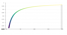
Capacitance doesn't seem to make much of a difference to duty time.
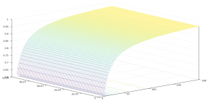
They always say ... be dumb, use a computer..
3618Kohm with 5nF should be correct..

Capacitance doesn't seem to make much of a difference to duty time.

They always say ... be dumb, use a computer..
3618Kohm with 5nF should be correct..
Last edited:
.. forward check = 89% at 86KHz switching rate.
The switching rate could come down a little - the current rate is giving 240V but isn't as strong.. so just waiting to see what the simulation gives.
The switching rate could come down a little - the current rate is giving 240V but isn't as strong.. so just waiting to see what the simulation gives.
The overnight run was a success with the 89% duty cycle, 84KHz and reduced current limit of 7.6A. The inductors are running at 2.8-3.4A each which is acceptable. The output from the supply sags about 10V when the 3080 regulator has fully warmed up, so I may opt to drop to 75Khz.
Updates to the PCB layout to accept the shielded transformer are coming along - I had to create a completely new footprint from scratch as component source didn't have one. When the parts arrive I'll measure it up vs the data sheet and double check the footprint.
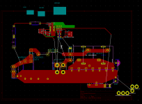
Given the current (and power) is now reduced a little it means I can target thinner tracks with 7-10A.
Updates to the PCB layout to accept the shielded transformer are coming along - I had to create a completely new footprint from scratch as component source didn't have one. When the parts arrive I'll measure it up vs the data sheet and double check the footprint.

Given the current (and power) is now reduced a little it means I can target thinner tracks with 7-10A.
Last edited:
Just tried a model with the UF diode, then realised it was the 600V variant (ie the 6 model) that's only available. Switched to an STM equiv part STTH310 (£0.56) which is a 1kV, 3A fast diode which has a model and it seems to be doing well so that's very much an option for that - I made the board able to take both foot prints for DO-201AD and TO220 packages. Needs a little retune given it's running at 85Khz still.
I've also made the board have footprints for both 80uF or 2x22uF caps - only difference is size and cost but if you a 3080 regulator after it doesn't make a difference. MKS4 900V 22uF is £5 a pop vs £20 for the 80uF. In reality a good bank of 4x22uF and an 80uF would be great but let's get the board working first. A separate 3080 board will sort minute additional ripple anyway.
It's happy as Larry running 580mA at 216V. Idea is tomorrow I'll finalise the BOM and put the remainder of the order in. I want to check the footprint sizes run it pass you folks and then I'll order a PCB.
Last edited:
- Home
- Amplifiers
- Power Supplies
- Tube use? 24->300V large cap charger with 300V 150mA reg
