The rest of us might be able to make sense of your readings if we knew how it was connected. And might be able to suggest resistor values for ones that are burnt beyond recognition.
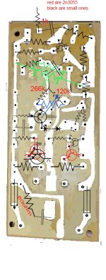
I tried making a schematic based on the image provided, but those wires from the 2N3055 are blocking the traces underneath it. It would help a lot if sg97 could take photos without these wires.Have we even attempted to trace out a schematic yet? This thing looks pretty simple.
I also created an image of the board with no components populated.
By the way, it looks like a 3D circuit combining P2P and PCB!
Last edited:

You only need 3 symbols. Resistors, capacitors and transistors. 🙂
https://www.diyaudio.com/community/...ing-after-shorting-output.406712/post-7556210
https://www.diyaudio.com/community/...ing-after-shorting-output.406712/post-7556210
my only issue is as you can see some componenct like resistors are not in pcb directly its connect in unusual way and how can i draw it in there ?
This is just an example, not the actual location of components.
Oh, and you'll need the diode symbol as well.

Oh, and you'll need the diode symbol as well.
i will do my best in showing where components are but as i said i may not able to draw all because not all components are on board its stupid and not professional. if it was board from commercial product it would be easier for me
as you can see there are some components outsire of board and also connected to eachother i will try to represent is as best as i can
i will add all components and label them as best as i can, btw for resistors caps and transistors i will use default symbols
sg97, that multimeter you have will not measure such low resistances accurately - even much better meters have trouble too. You'd need a meter that can specifically measure milliohms, and they're not cheap.yes it does. so i measure like from 00.6 to 01 something
That is progress 🙂, but there are things that don''t make sense to me. I dont have much time right now, but to start:
the two diodes with the resistor in series, I think they are the bias parts. The driver transistors (the small ones that have one leg connected to the base of a 2n3055) should have their base connected to the bias string, one on either side. But I don't see that in your picture, so I am confused..
the two diodes with the resistor in series, I think they are the bias parts. The driver transistors (the small ones that have one leg connected to the base of a 2n3055) should have their base connected to the bias string, one on either side. But I don't see that in your picture, so I am confused..
trust me all the parts except two resistors i changed are there even when it was working 2 years ago. i am not sure what can cause problems it looks really messy
for red resistors i marked 2n3055 i am 90% sure it is like that for small ones i am not really sure of e c and b but connection points are right
btw that big cap there appears to be shorted with a wire ? it does not connect to anything now its shorted
- Home
- Amplifiers
- Solid State
- transistor amp not working after shorting output