DC voltage range on your meter for all the rails, not AC 🙂
For now we'll say the 30vdc is OK on the right channel. The positive rail should be a little higher than that value.
Left channel need a bit of old fashioned fault finding. You've built both up identically and so both should perform the same. Perhaps some open print somewhere around the pads of one of the transistors.
Be extremely careful not to short anything when measuring... its easily done.
So the left channel... look at the simulation I posted above for voltages. Do you see how nearly the same voltage appears all the way through the circuit in this state. You need to see where yours is missing.
1/ Check you have positive supply voltage on R18 and R16. You should see the voltage carried through to each leg of each resistor.
R18 = -19.3 and -32.2
R16 = -19.3 and -00.9
2/ That same voltage should appear on the 150 ohm less a little bit.
-00.4 and +00.4
3/ The voltage on the 150 ohm should appear on the emitter of the NPN output transistor TR12
Not seeing any voltage at the emitter of TR12 🙁
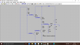
Like this. Begin with 'A' and work through measuring at each point. You should see the same voltage carried through all the way to F.
I think the negative values are down to this meter, I have the black probe to ground but getting (-) results. I did the same checks on the other channel right channel and the results where more or less what you said they should be but still reading negative.
Working on one just one channel would be easier rather than having both on the go 🙂
Nothing should generate any heat at all at this stage apart from R17 and R15 and then only if TR5 was fitted. Other reference numbers for the other channel of course.
The wire link between the driver bases means that no voltage difference can appear between them and that means no current can flow in them. That condition is absolute and fixed.
Although one or the other driver transistor may be on, they can not both be on together. The link forces that condition and that means they all run cold.
So the heat generation in TR9 means there is a problem with either the parts or the fitting of them. Current is flowing that shouldn't.
Although TR6 should be out of circuit it would not cause any overheating of the drivers or outputs no matter what condition/fault etc that particular transistor (TR6) may have... at least if there are no problems with the driver/outputs.
Just when it all seemed to be going so well 😱
Check visually that you really have got those transistors fitted correctly... compare with the channel that is cold. Make sure the BD139 is fitted for TR7 and the BD140 for TR9. Collector is the middle leg, make sure E and B are correctly positioned.
You need to prove the meter is reading correctly. Meter leads the right way around at the meter itself?
With the black lead on ground you should read PLUS supply on at least one end of R18 (one end goes direct to the PLUS rails)
Keeping the black lead on ground you should read MINUS supply on at least one end of R51 (one end goes direct to the MINUS rail)
With the black lead on ground you should read PLUS supply on at least one end of R18 (one end goes direct to the PLUS rails)
Keeping the black lead on ground you should read MINUS supply on at least one end of R51 (one end goes direct to the MINUS rail)
Last one for tonight.
You have to reach this state. If this is correct then nothing in front of this stage can cause any current to flow in the transistors. Its a 'safe' configuration.
Make sure TR9 B and E are not reversed (and TR7 8, and TR10).
You have to reach this state. If this is correct then nothing in front of this stage can cause any current to flow in the transistors. Its a 'safe' configuration.
Make sure TR9 B and E are not reversed (and TR7 8, and TR10).
Attachments
You need to prove the meter is reading correctly. Meter leads the right way around at the meter itself?
With the black lead on ground you should read PLUS supply on at least one end of R18 (one end goes direct to the PLUS rails)
Keeping the black lead on ground you should read MINUS supply on at least one end of R51 (one end goes direct to the MINUS rail)
Had swapped the leads around on the tester so all those minus reads are in fact positive...
R51 reads neg 32.2 and neg 32.4 between ground and each leg
Last edited:
Last one for tonight.
You have to reach this state. If this is correct then nothing in front of this stage can cause any current to flow in the transistors. Its a 'safe' configuration.
Make sure TR9 B and E are not reversed (and TR7 8, and TR10).
they're definitely right, ECB in the right places.


Thanks for the picture. Having the pinouts marked on the board makes it easier.
OK, another day... lets try and crack this one by working on just one channel.
The theory is rock solid and sound and so when things aren't as they should be it means there is a definite and real problem.
So lets start with this obvious problem and just go back on the theory of what should happen:
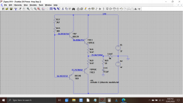
This is the configuration you have (attached). R17 fitted. TR5 removed. TR9 getting hot.
This is what should happen:
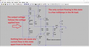
R17 and R15 apply the positive rail voltage to the driver transistor base's.
TR7 and TR11 are now biased 'on' but there is nowhere for any current to flow apart from into the load resistor (9k). Because they are 'on' you see almost the full positive rail voltage at the output.
TR9 and TR13 are most definitely 'off' in this state and neither passes any current at all.
So why is TR9 hot?
And this is where fault finding is so interesting 🙂 it's all about pulling in evidence and looking for reasons why something might be wrong.
We know we have positive supply voltage at the output terminal.
TR13 base will also see that voltage because the E-B junction behaves like a forward biased diode putting this same voltage onto TR9 emitter.
So far so good... but TR9 should definitely be fully off as it is configured. Off means cold.
A bit more evidence is needed to try and piece this part of the puzzle together.
Current flows will leave a trail by means of the volt drop they create across the resistors.
Other possibilities to check/confirm:
1/ Were the driver transistors new and unused and from a reputable source?
2/ Check by measurement (continuity test with amp off) that the actual Base, Emitter and Collector of each driver goes where it is supposed to on the board. Although unlikely it can happen that board markings are wrong.
So look at the data sheet for the BD140 and make sure that the middle lead connects to R51 and that the 150 ohm connects to the emitter.
Now make sure that the base of the BD140 itself connects to the base of the BD139 (it should do as they are linked by wire).
Above all don't lose sight of the fact that the problem at this point in this channel has to be around those transistors or a problem with them.
The attached image shows the configuration we should be in. You should have no voltage across (measured now across) either of those 22 ohm resistors and also no voltage across the 150 ohm.
OK, another day... lets try and crack this one by working on just one channel.
The theory is rock solid and sound and so when things aren't as they should be it means there is a definite and real problem.
So lets start with this obvious problem and just go back on the theory of what should happen:
Ok, Mooly clearer what to do now. Just to note, the diagram says point A is R17 which is the other channel. Should I just follow the same path on the left using the equivalent components? Also, TR9 seems to be getting real hot. TR10 less so but I can feel heat on it.
Also, TR5 was removed from the right channel when R17 was put back but on the other side everything is in circuit. I didn't remove TR6, was I supposed to?
Thanks
This is the configuration you have (attached). R17 fitted. TR5 removed. TR9 getting hot.
This is what should happen:
R17 and R15 apply the positive rail voltage to the driver transistor base's.
TR7 and TR11 are now biased 'on' but there is nowhere for any current to flow apart from into the load resistor (9k). Because they are 'on' you see almost the full positive rail voltage at the output.
TR9 and TR13 are most definitely 'off' in this state and neither passes any current at all.
So why is TR9 hot?
And this is where fault finding is so interesting 🙂 it's all about pulling in evidence and looking for reasons why something might be wrong.
We know we have positive supply voltage at the output terminal.
TR13 base will also see that voltage because the E-B junction behaves like a forward biased diode putting this same voltage onto TR9 emitter.
So far so good... but TR9 should definitely be fully off as it is configured. Off means cold.
A bit more evidence is needed to try and piece this part of the puzzle together.
Current flows will leave a trail by means of the volt drop they create across the resistors.
Other possibilities to check/confirm:
1/ Were the driver transistors new and unused and from a reputable source?
2/ Check by measurement (continuity test with amp off) that the actual Base, Emitter and Collector of each driver goes where it is supposed to on the board. Although unlikely it can happen that board markings are wrong.
So look at the data sheet for the BD140 and make sure that the middle lead connects to R51 and that the 150 ohm connects to the emitter.
Now make sure that the base of the BD140 itself connects to the base of the BD139 (it should do as they are linked by wire).
Above all don't lose sight of the fact that the problem at this point in this channel has to be around those transistors or a problem with them.
The attached image shows the configuration we should be in. You should have no voltage across (measured now across) either of those 22 ohm resistors and also no voltage across the 150 ohm.
Attachments
Just digesting that lot, Mooly. Cheers.
Will crack on with that but just had a thought. I've got the Bases linked but still in circuit. Should they be linked together but not soldered down or is it ok linked but still in circuit how I have them?
Will crack on with that but just had a thought. I've got the Bases linked but still in circuit. Should they be linked together but not soldered down or is it ok linked but still in circuit how I have them?
You've got it, they stay in circuit and connected to R15/17.
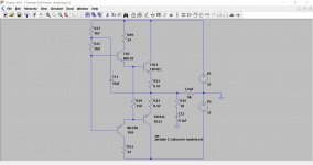
Without wanting to confuse you, this is how the circuit reduces down to it's fundamental parts. The speaker output follows the base voltage of the drivers, no matter what the polarity.
With no load attached no measurable current (for our purposes) flows in any component in this state.
If we linked R17 to the negative rail (second image) the voltages all reverse polarity. Again no current flows anywhere.
Check for any solder blobs anywhere around those transistors.
Attachments
1/ Were the driver transistors new and unused and from a reputable source?
They where from the same source as the last lot which worked but I thought lacked bass. I had the BD140's left over but had to re-order the 139's.
I have just tested all the BD140's and BD139's I have, some have been fitted and then lifted, one, a BD139 tested bad, the rest tested ok. That bad one I expect is the one which had been in the channel which smoked when I put R17 back by mistake. The ones which where used but tested ok would have been from the other channel as I replaced all 4 drivers for fresh ones when I installed the output transistors.
2/ Check by measurement (continuity test with amp off) that the actual Base, Emitter and Collector of each driver goes where it is supposed to on the board. Although unlikely it can happen that board markings are wrong.
I have checked that they all go where they are meant to on the schematic and tested for continuity but found no open circuit. All seems how it should. I also scrutinised all the traces around the transistor legs solder points for blobs of solder but all seem fine.
I tested the drivers which are in the amp now and found BD139 to be bad. I'm guessing something caused this to go bad since it went 'in circuit' as it was a new unused transistor.....
These where the results:
[
B]TR7 (BD139)
[/B]
Step 1: (Base to Emitter)
Hook the positive lead from the multimeter to the to the BASE (B) of the transistor. Hook the negative meter lead to the EMITTER (E) of the transistor. For an good NPN transistor, the meter should show a voltage drop between 0.45V and 0.9V. If you are testing PNP transistor, you should see “OL” (Over Limit).
814
Step 2: (Base to Collector)
Keep the postitive lead on the BASE (B) and place the negative lead to the COLLECTOR (C).
For an good NPN transistor, the meter should show a voltage drop between 0.45V and 0.9V. If you are testing PNP transistor, you should see "OL" (Over Limit).
814
Step 3: (Emitter to Base)
Hook the positive lead from the multimeter to the to the EMITTER (E) of the transistor. Hook the negative meter lead to the BASE (B) of the transistor.
For an good NPN transistor, you should see “OL” (Over Limit).If you are testing PNP transistor, the meter should show a voltage drop between 0.45V and 0.9V.
642
Step 4: (Collector to Base)
Hook the positive lead from the multimeter to the to the COLLECTOR (C) of the transistor. Hook the negative meter lead to the BASE (B) of the transistor.
For an good NPN transistor, you should see “OL” (Over Limit).If you are testing PNP transistor, the meter should show a voltage drop between 0.45V and 0.9V.
OL
Step 5: (Collector to Emitter)
Hook the postitive meter lead to the COLLECTOR (C) and the negative meter lead to the EMITTER (E) – A good NPN or PNP transistor will read "OL"/Over Limit on the meter.
699
Swap the leads (Positive to Emitter and Negative to Collector) – Once again, a good NPN or PNP transistor should read “OL”.
641
So, If I replace TR7 with a fresh BD139 which I've tested out of circuit, will that malfunction after being energised? If so, what might be causing it?
I didn't test it prior to fitting, what are the odds that I had a dud to start with?
Thanks.
Tested TR8 (BD139)
Step 1: (Base to Emitter)
814
Step 2: (Base to Collector)
812
Step 3: (Emitter to Base)
OL
Step 4: (Collector to Base)
OL
Step 5: (Collector to Emitter)
702
Positive to Emitter and Negative to Collector
649
😕
Step 1: (Base to Emitter)
814
Step 2: (Base to Collector)
812
Step 3: (Emitter to Base)
OL
Step 4: (Collector to Base)
OL
Step 5: (Collector to Emitter)
702
Positive to Emitter and Negative to Collector
649
😕
Tested TR9 (BD140)
Step 1: (Base to Emitter)
1006
Step 2: (Base to Collector)
OL
Step 3: (Emitter to Base)
780
Step 4: (Collector to Base)
780
Step 5: (Collector to Emitter)
660
Positive to Emitter and Negative to Collector
OL
Step 1: (Base to Emitter)
1006
Step 2: (Base to Collector)
OL
Step 3: (Emitter to Base)
780
Step 4: (Collector to Base)
780
Step 5: (Collector to Emitter)
660
Positive to Emitter and Negative to Collector
OL
Tested Tr10 (BD140)
Step 1: (Base to Emitter)
OL
Step 2: (Base to Collector)
OL
Step 3: (Emitter to Base)
780
Step 4: (Collector to Base)
779
Step 5: (Collector to Emitter)
703 😕
Positive to Emitter and Negative to Collector
OL
Step 1: (Base to Emitter)
OL
Step 2: (Base to Collector)
OL
Step 3: (Emitter to Base)
780
Step 4: (Collector to Base)
779
Step 5: (Collector to Emitter)
703 😕
Positive to Emitter and Negative to Collector
OL
- Home
- Amplifiers
- Solid State
- Toshiba 330 power amp